PIC24FJ64GA104 FAMILY
REGISTER 14-2: OCxCON2: OUTPUT COMPARE x CONTROL REGISTER 2 (CONTINUED)
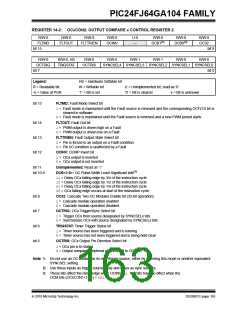
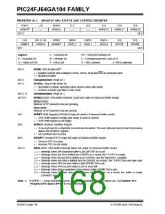
bit 4-0
SYNCSEL<4:0>: Trigger/Synchronization Source Selection bits
11111= This OC module(1)
11110= Reserved
11101= Reserved
11100= CTMU(2)
11011= A/D(2)
11010= Comparator 3(2)
11001= Comparator 2(2)
11000= Comparator 1(2)
10111= Input Capture 4(2)
10110= Input Capture 3(2)
10101= Input Capture 2(2)
10100= Input Capture 1(2)
100xx= Reserved
01111= Timer5
01110= Timer4
01101= Timer3
01100= Timer2
01011= Timer1
01010= Input Capture 5(2)
01001= Reserved
01000= Reserved
00111= Reserved
00110= Reserved
00101= Output Compare 5(1)
00100= Output Compare 4(1)
00011= Output Compare 3(1)
00010= Output Compare 2(1)
00001= Output Compare 1(1)
00000= Not synchronized to any other module
Note 1: Do not use an OC module as its own trigger source, either by selecting this mode or another equivalent
SYNCSEL setting.
2: Use these inputs as trigger sources only and never as sync sources.
3: These bits affect the rising edge when OCINV = 1. The bits have no effect when the
OCM bits (OCxCON1<1:0>) = 001.
DS39951C-page 164
2010 Microchip Technology Inc.

 MICROCHIP [ MICROCHIP ]