PIC24FJ64GA104 FAMILY
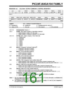
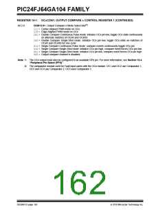
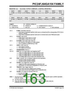
REGISTER 14-2: OCxCON2: OUTPUT COMPARE x CONTROL REGISTER 2
R/W-0
R/W-0
R/W-0
R/W-0
U-0
—
R/W-0
DCB1(3)
R/W-0
DCB0(3)
R/W-0
OC32
FLTMD
FLTOUT
FLTTRIEN
OCINV
bit 15
bit 8
R/W-0
R/W-0, HS
TRIGSTAT
R/W-0
R/W-0
R/W-1
R/W-1
R/W-0
R/W-0
OCTRIG
OCTRIS
SYNCSEL4 SYNCSEL3 SYNCSEL2 SYNCSEL1 SYNCSEL0
bit 0
bit 7
Legend:
HS = Hardware Settable bit
W = Writable bit
R = Readable bit
-n = Value at POR
U = Unimplemented bit, read as ‘0’
‘0’ = Bit is cleared x = Bit is unknown
‘1’ = Bit is set
bit 15
FLTMD: Fault Mode Select bit
1= Fault mode is maintained until the Fault source is removed and the corresponding OCFLT0 bit is
cleared in software
0= Fault mode is maintained until the Fault source is removed and a new PWM period starts
bit 14
bit 13
bit 12
FLTOUT: Fault Out bit
1= PWM output is driven high on a Fault
0= PWM output is driven low on a Fault
FLTTRIEN: Fault Output State Select bit
1= Pin is forced to an output on a Fault condition
0= Pin I/O condition is unaffected by a Fault
OCINV: OCMP Invert bit
1= OCx output is inverted
0= OCx output is not inverted
bit 11
Unimplemented: Read as ‘0’
bit 10-9
DCB<1:0>: OC Pulse-Width Least Significant bits(3)
11= Delay OCx falling edge by 3/4 of the instruction cycle
10= Delay OCx falling edge by 1/2 of the instruction cycle
01= Delay OCx falling edge by 1/4 of the instruction cycle
00= OCx falling edge occurs at start of the instruction cycle
bit 8
bit 7
bit 6
bit 5
OC32: Cascade Two OC Modules Enable bit (32-bit operation)
1= Cascade module operation enabled
0= Cascade module operation disabled
OCTRIG: OCx Trigger/Sync Select bit
1= Trigger OCx from source designated by SYNCSELx bits
0= Synchronize OCx with source designated by SYNCSELx bits
TRIGSTAT: Timer Trigger Status bit
1= Timer source has been triggered and is running
0= Timer source has not been triggered and is being held clear
OCTRIS: OCx Output Pin Direction Select bit
1= OCx pin is tri-stated
0= Output compare peripheral x connected to OCx pin
Note 1: Do not use an OC module as its own trigger source, either by selecting this mode or another equivalent
SYNCSEL setting.
2: Use these inputs as trigger sources only and never as sync sources.
3: These bits affect the rising edge when OCINV = 1. The bits have no effect when the
OCM bits (OCxCON1<1:0>) = 001.
2010 Microchip Technology Inc.
DS39951C-page 163

 MICROCHIP [ MICROCHIP ]