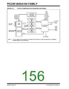
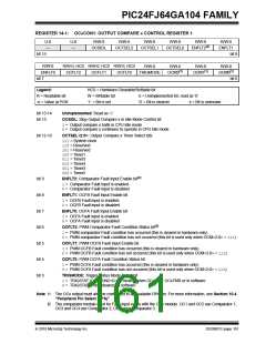
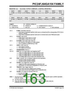
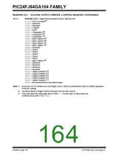
PIC24FJ64GA104 FAMILY
The DCB bits are intended for use with a clock source
14.4 Subcycle Resolution
identical to the system clock. When an OCx module
with enabled prescaler is used, the falling edge delay
caused by the DCB bits will be referenced to the
system clock period, rather than the OCx module's
period.
The DCB bits (OCxCON2<10:9>) provide for resolution
better than one instruction cycle. When used, they
delay the falling edge generated by a match event by a
portion of an instruction cycle.
For example, setting DCB<1:0> = 10causes the falling
edge to occur half way through the instruction cycle in
which the match event occurs, instead of at the
beginning. These bits cannot be used when
OCM<2:0> = 001. When operating the module in PWM
mode (OCM<2:0> = 110or 111), the DCB bits will be
double-buffered.
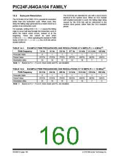
TABLE 14-1: EXAMPLE PWM FREQUENCIES AND RESOLUTIONS AT 4 MIPS (FCY = 4 MHz)(1)
PWM Frequency
Prescaler Ratio
7.6 Hz
61 Hz
122 Hz
977 Hz
3.9 kHz
31.3 kHz
125 kHz
8
1
FFFFh
16
1
1
1
1
007Fh
7
1
001Fh
5
Period Value
FFFFh
16
7FFFh
15
0FFFh
12
03FFh
10
Resolution (bits)
Note 1: Based on FCY = FOSC/2; Doze mode and PLL are disabled.
TABLE 14-2: EXAMPLE PWM FREQUENCIES AND RESOLUTIONS AT 16 MIPS (FCY = 16 MHz)(1)
PWM Frequency
Prescaler Ratio
30.5 Hz
244 Hz
488 Hz
3.9 kHz
15.6 kHz
125 kHz
500 kHz
8
1
FFFFh
16
1
1
1
1
007Fh
7
1
001Fh
5
Period Value
FFFFh
16
7FFFh
15
0FFFh
12
03FFh
10
Resolution (bits)
Note 1: Based on FCY = FOSC/2; Doze mode and PLL are disabled.
DS39951C-page 160
2010 Microchip Technology Inc.

 MICROCHIP [ MICROCHIP ]