PIC24FJ64GA104 FAMILY
To set up the SPI module for the Standard Master mode
of operation:
To set up the SPI module for the Standard Slave mode
of operation:
1. If using interrupts:
1. Clear the SPIxBUF register.
2. If using interrupts:
a) Clear the SPIxIF bit in the respective IFS
register.
a) Clear the SPIxIF bit in the respective IFS
register.
b) Set the SPIxIE bit in the respective IEC
register.
b) Set the SPIxIE bit in the respective IEC
register.
c) Write the SPIxIP bits in the respective IPC
register to set the interrupt priority.
c) Write the SPIxIP bits in the respective IPC
register to set the interrupt priority.
2. Write the desired settings to the SPIxCON1
and SPIxCON2 registers with MSTEN
(SPIxCON1<5>) = 1.
3. Write the desired settings to the SPIxCON1
and SPIxCON2 registers with MSTEN
(SPIxCON1<5>) = 0.
3. Clear the SPIROV bit (SPIxSTAT<6>).
4. Enable SPI operation by setting the SPIEN bit
(SPIxSTAT<15>).
4. Clear the SMP bit.
5. If the CKE bit (SPIxCON1<8>) is set, then the
SSEN bit (SPIxCON1<7>) must be set to enable
the SSx pin.
5. Write the data to be transmitted to the SPIxBUF
register. Transmission (and reception) will start
as soon as data is written to the SPIxBUF
register.
6. Clear the SPIROV bit (SPIxSTAT<6>).
7. Enable SPI operation by setting the SPIEN bit
(SPIxSTAT<15>).
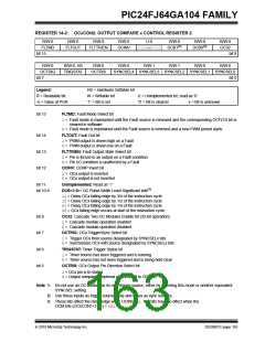
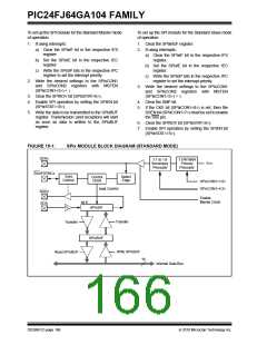
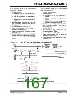
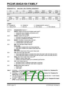
FIGURE 15-1:
SPIx MODULE BLOCK DIAGRAM (STANDARD MODE)
SCKx
1:1 to 1:8
Secondary
Prescaler
1:1/4/16/64
Primary
Prescaler
FCY
SSx/FSYNCx
Sync
Control
Select
Edge
Control
Clock
SPIxCON1<1:0>
SPIxCON1<4:2>
Control
Shift
SDOx
SDIx
Enable
Master Clock
bit 0
SPIxSR
Transfer
Transfer
SPIxBUF
Write SPIxBUF
Read SPIxBUF
16
Internal Data Bus
DS39951C-page 166
2010 Microchip Technology Inc.

 MICROCHIP [ MICROCHIP ]