PIC24FJ64GA104 FAMILY
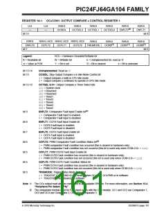
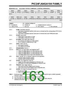
REGISTER 14-1: OCxCON1: OUTPUT COMPARE x CONTROL REGISTER 1
U-0
—
U-0
—
R/W-0
R/W-0
R/W-0
R/W-0
R/W-0
ENFLT2(2)
R/W-0
OCSIDL
OCTSEL2
OCTSEL1
OCTSEL0
ENFLT1
bit 15
bit 8
R/W-0
R/W-0, HCS R/W-0, HCS R/W-0, HCS
OCFLT2 OCFLT1 OCFLT0
R/W-0
R/W-0
OCM2(1)
R/W-0
OCM1(1)
R/W-0
OCM0(1)
ENFLT0
TRIGMODE
bit 7
bit 0
Legend:
HCS = Hardware Clearable/Settable bit
R = Readable bit
W = Writable bit
‘1’ = Bit is set
U = Unimplemented bit, read as ‘0’
‘0’ = Bit is cleared x = Bit is unknown
-n = Value at POR
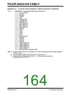
bit 15-14
bit 13
Unimplemented: Read as ‘0’
OCSIDL: Stop Output Compare x in Idle Mode Control bit
1= Output compare x halts in CPU Idle mode
0= Output compare x continues to operate in CPU Idle mode
bit 12-10
OCTSEL<2:0>: Output Compare x Timer Select bits
111= System clock
110= Reserved
101= Reserved
100= Timer1
011= Timer5
010= Timer4
001= Timer3
000= Timer2
bit 9
bit 8
bit 7
bit 6
bit 5
bit 4
bit 3
ENFLT2: Comparator Fault Input Enable bit(2)
1= Comparator Fault input is enabled
0= Comparator Fault input is disabled
ENFLT1: OCFB Fault Input Enable bit
1= OCFB Fault input is enabled
0= OCFB Fault input is disabled
ENFLT0: OCFA Fault Input Enable bit
1= OCFA Fault input is enabled
0= OCFA Fault input is disabled
OCFLT2: PWM Comparator Fault Condition Status bit(2)
1= PWM comparator Fault condition has occurred (this is cleared in hardware only)
0= PWM comparator Fault condition has not occurred (this bit is used only when OCM<2:0> = 111)
OCFLT1: PWM OCFB Fault Input Enable bit
1= PWM OCFB Fault condition has occurred (this is cleared in hardware only)
0= PWM OCFB Fault condition has not occurred (this bit is used only when OCM<2:0> = 111)
OCFLT0: PWM OCFA Fault Condition Status bit
1= PWM OCFA Fault condition has occurred (this is cleared in hardware only)
0= PWM OCFA Fault condition has not occurred (this bit is used only when OCM<2:0> = 111)
TRIGMODE: Trigger Status Mode Select bit
1= TRIGSTAT (OCxCON2<6>) is cleared when OCxRS = OCxTMR or in software
0= TRIGSTAT is only cleared by software
Note 1: The OCx output must also be configured to an available RPn pin. For more information, see Section 10.4
“Peripheral Pin Select (PPS)”.
2: The comparator module used for Fault input varies with the OCx module. OC1 and OC2 use Comparator 1;
OC3 and OC4 use Comparator 2; OC5 uses Comparator 3.
2010 Microchip Technology Inc.
DS39951C-page 161

 MICROCHIP [ MICROCHIP ]