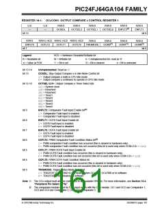
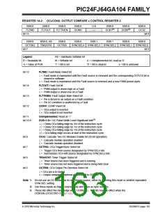
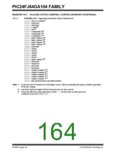
PIC24FJ64GA104 FAMILY
The SPI serial interface consists of four pins:
15.0 SERIAL PERIPHERAL
INTERFACE (SPI)
• SDIx: Serial Data Input
• SDOx: Serial Data Output
• SCKx: Shift Clock Input or Output
Note:
This data sheet summarizes the features
of this group of PIC24F devices. It is not
• SSx: Active-Low Slave Select or Frame
Synchronization I/O Pulse
intended to be a comprehensive reference
source. For more information, refer to the
“PIC24F Family Reference Manual”,
Section 23. “Serial Peripheral Interface
(SPI)” (DS39699).
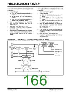
The SPI module can be configured to operate using
2, 3 or 4 pins. In the 3-pin mode, SSx is not used. In the
2-pin mode, both SDOx and SSx are not used.
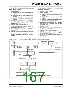
Block diagrams of the module in Standard and
Enhanced modes are shown in Figure 15-1 and
Figure 15-2.
The Serial Peripheral Interface (SPI) module is a
synchronous serial interface useful for communicating
with other peripheral or microcontroller devices. These
peripheral devices may be serial EEPROMs, shift
registers, display drivers, A/D Converters, etc. The SPI
module is compatible with Motorola® SPI and SIOP
interfaces. All devices of the PIC24FJ64GA104 family
include three SPI modules
Note:
In this section, the SPI modules are
referred to together as SPIx or separately
as SPI1, SPI2 or SPI3. Special Function
Registers will follow a similar notation. For
example, SPIxCON1 and SPIxCON2 refer
to the control registers for any of the 3 SPI
modules.
The module supports operation in two buffer modes. In
Standard mode, data is shifted through a single serial
buffer. In Enhanced Buffer mode, data is shifted
through an 8-level FIFO buffer.
Note:
Do not perform read-modify-write opera-
tions (such as bit-oriented instructions) on
the SPIxBUF register in either Standard or
Enhanced Buffer mode.
The module also supports a basic framed SPI protocol
while operating in either Master or Slave mode. A total
of four framed SPI configurations are supported.
2010 Microchip Technology Inc.
DS39951C-page 165

 MICROCHIP [ MICROCHIP ]