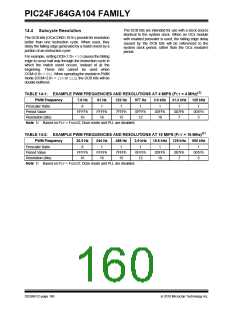
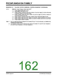
PIC24FJ64GA104 FAMILY
5. Select
a clock source by writing to the
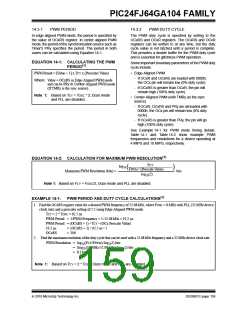
14.3 Pulse-Width Modulation (PWM)
Mode
OCTSEL2<2:0> (OCxCON1<12:10>) bits.
6. Enable interrupts, if required, for the timer and
output compare modules. The output compare
interrupt is required for PWM Fault pin utilization.
In PWM mode, the output compare module can be
configured for edge-aligned or center-aligned pulse
waveform generation. All PWM operations are
double-buffered (buffer registers are internal to the
module and are not mapped into SFR space).
7. Select the desired PWM mode in the OCM<2:0>
(OCxCON1<2:0>) bits.
8. If a timer is selected as a clock source, set the
TMRy prescale value and enable the time base by
setting the TON (TxCON<15>) bit.
To configure the output compare module for
edge-aligned PWM operation:
Note:
This peripheral contains input and output
functions that may need to be configured
by the Peripheral Pin Select. See
Section 10.4 “Peripheral Pin Select
(PPS)” for more information.
1. Configure the OCx output for one of the
available Peripheral Pin Select pins.
2. Calculate the desired on-time and load it into the
OCxR register.
3. Calculate the desired period and load it into the
OCxRS register.
4. Select the current OCx as the synchronization
source by writing 0x1F to SYNCSEL<4:0>
(OCxCON2<4:0>) and ‘0’ to OCTRIG
(OCxCON2<7>).
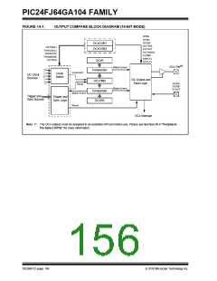
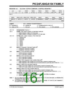
FIGURE 14-2:
OUTPUT COMPARE BLOCK DIAGRAM
(DOUBLE-BUFFERED, 16-BIT PWM MODE)
OCxCON1
OCxCON2
OCMx
OCINV
OCTSELx
OCTRIS
FLTOUT
FLTTRIEN
FLTMD
SYNCSELx
TRIGSTAT
TRIGMODE
OCTRIG
OCxR and DCB<1:0>
Rollover/Reset
ENFLTx
OCFLTx
DCB<1:0>
OCxR and DCB<1:0> Buffers
(1)
OCx Pin
Comparator
Match
Event
Increment
Clock
Select
OC Clock
Sources
OC Output Timing
and Fault Logic
OCxTMR
Comparator
OCxRS Buffer
Rollover
Reset
OCFA/OCFB/CxOUT
Match
Event
Match Event
Trigger and
Sync Logic
Trigger and
Sync Sources
Rollover/Reset
OCxRS
OCx Interrupt
Reset
Note 1: The OCx outputs must be assigned to an available RPn pin before use. Please see Section 10.4 “Peripheral Pin
Select (PPS)” for more information.
DS39951C-page 158
2010 Microchip Technology Inc.

 MICROCHIP [ MICROCHIP ]