PIC24FJ64GA104 FAMILY
For 32-bit cascaded operation, these steps are also
necessary:
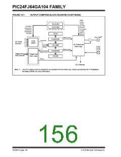
14.2 Compare Operations
In Compare mode (Figure 14-1), the output compare
module can be configured for single-shot or continuous
pulse generation; it can also repeatedly toggle an
output pin on each timer event.
1. Set the OC32 bits for both registers
(OCyCON2<8> and (OCxCON2<8>). Enable
the even-numbered module first to ensure the
modules will start functioning in unison.
To set up the module for compare operations:
2. Clear the OCTRIG bit of the even module
(OCyCON2), so the module will run in
Synchronous mode.
1. Configure the OCx output for one of the
available Peripheral Pin Select pins.
2. Calculate the required values for the OCxR and
(for Double Compare modes) OCxRS Duty Cycle
registers:
3. Configure the desired output and Fault settings
for OCy.
4. Force the output pin for OCx to the output state
by clearing the OCTRIS bit.
a) Determine the instruction clock cycle time.
Take into account the frequency of the
external clock to the timer source (if one is
used) and the timer prescaler settings.
5. If Trigger mode operation is required, configure
the trigger options in OCx by using the OCTRIG
(OCxCON2<7>), TRIGSTAT (OCxCON2<6>)
and SYNCSEL (OCxCON2<4:0>) bits.
b) Calculate time to the rising edge of the
output pulse relative to the timer start value
(0000h).
6. Configure the desired Compare or PWM mode
of operation (OCM<2:0>) for OCy first, then for
OCx.
c) Calculate the time to the falling edge of the
pulse based on the desired pulse width and
the time to the rising edge of the pulse.
Depending on the output mode selected, the module
holds the OCx pin in its default state and forces a
transition to the opposite state when OCxR matches
the timer. In Double Compare modes, OCx is forced
back to its default state when a match with OCxRS
occurs. The OCxIF interrupt flag is set after an OCxR
match in Single Compare modes and after each
OCxRS match in Double Compare modes.
3. Write the rising edge value to OCxR and the
falling edge value to OCxRS.
4. For Trigger mode operations, set OCTRIG to
enable Trigger mode. Set or clear TRIGMODE to
configure trigger operation and TRIGSTAT to
select a hardware or software trigger. For
Synchronous mode, clear OCTRIG.
Single-shot pulse events only occur once, but may be
repeated by simply rewriting the value of the
OCxCON1 register. Continuous pulse events continue
indefinitely until terminated.
5. Set the SYNCSEL<4:0> bits to configure the
trigger or synchronization source. If free-running
timer operation is required, set the SYNCSEL
bits to ‘00000’ (no sync/trigger source).
6. Select the time base source with the
OCTSEL<2:0> bits. If the desired clock source is
running, set the OCTSEL<2:0> bits before the
output compare module is enabled for proper
synchronization with the desired clock source. If
necessary, set the TON bit for the selected timer
which enables the compare time base to count.
Synchronous mode operation starts as soon as
the synchronization source is enabled. Trigger
mode operation starts after a trigger source event
occurs.
7. Set the OCM<2:0> bits for the appropriate
compare operation (= 0xx).
2010 Microchip Technology Inc.
DS39951C-page 157

 MICROCHIP [ MICROCHIP ]