PIC17C75X
13.1.3.3 EXTERNAL CLOCK SOURCE
13.1.3.3.1 MAX RESOLUTION/FREQUENCY FOR
EXTERNAL CLOCK INPUT
The PWMs will operate regardless of the clock source
of the timer. The use of an external clock has ramifica-
tions that must be understood. Because the external
TCLK12 input is synchronized internally (sampled once
per instruction cycle), the time TCLK12 changes to the
time the timer increments will vary by as much as 1TCY
(one instruction cycle). This will cause jitter in the duty
cycle as well as the period of the PWM output.
The use of an external clock for the PWM time-base
(Timer1 or Timer2) limits the PWM output to a maxi-
mum resolution of 8-bits. The PWxDCL<7:6> bits must
be kept cleared. Use of any other value will distort the
PWM output. All resolutions are supported when inter-
nal clock mode is selected. The maximum attainable
frequency is also lower. This is a result of the timing
requirements of an external clock input for a timer (see
the Electrical Specification section). The maximum
PWM frequency, when the timers clock source is the
RB4/TCLK12 pin, as shown in Table 13-4 (standard
resolution mode).
This jitter will be ±1TCY, unless the external clock is
synchronized with the processor clock. Use of one of
the PWM outputs as the clock source to the TCLK12
input, will supply a synchronized clock.
In general, when using an external clock source for
PWM, its frequency should be much less than the
device frequency (Fosc).
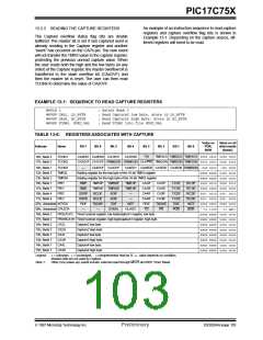
TABLE 13-5: REGISTERS/BITS ASSOCIATED WITH PWM
Value on all
other
resets
Value on
POR,
BOR
Address
Name
Bit 7
Bit 6
Bit 5
Bit 4
Bit 3
Bit 2
Bit 1
Bit 0
(Note1)
16h, Bank 3
17h, Bank 3
TCON1
TCON2
CA2ED1
CA2OVF
—
CA2ED0
CA1ED1
CA1ED0
T16
TMR3CS TMR2CS TMR1CS 0000 0000 0000 0000
CA1OVF PWM2ON PWM1ON CA1/PR3 TMR3ON TMR2ON TMR1ON 0000 0000 0000 0000
16h, Bank 7
10h, Bank 2
11h, Bank 2
16h, Bank 1
17h, Bank 1
TCON3
TMR1
TMR2
PIR1
CA4OVF
CA3OVF
CA4ED1
CA4ED0 CA3ED1 CA3ED0 PWM3ON -000 0000 -000 0000
xxxx xxxx uuuu uuuu
Timer1’s register
Timer2’s register
xxxx xxxx uuuu uuuu
RBIF
RBIE
PEIF
TMR3IF
TMR2IF
TMR2IE
T0IF
TMR1IF
TMR1IE
INTF
CA2IF
CA2IE
PEIE
CA1IF
CA1IE
TX1IF
TX1IE
T0IE
RC1IF
RC1IE
INTE
0000 0010 0000 0010
0000 0000 0000 0000
0000 0000 0000 0000
PIE1
TMR3IE
T0CKIF
07h, Unbanked INTSTA
06h, Unbanked CPUSTA
T0CKIE
—
—
STKAV
GLINTD
TO
PD
POR
BOR
--11 1100 --11 qq11
xxxx xxxx uuuu uuuu
xxxx xxxx uuuu uuuu
xx-- ---- uu-- ----
xx0- ---- uu0- ----
xx0- ---- uu0- ----
xxxx xxxx uuuu uuuu
xxxx xxxx uuuu uuuu
xxxx xxxx uuuu uuuu
14h, Bank 2
15h, Bank 2
10h, Bank 3
11h, Bank 3
10h, Bank 7
12h, Bank 3
13h, Bank 3
11h, Bank 7
PR1
Timer1 period register
Timer2 period register
PR2
PW1DCL
PW2DCL
PW3DCL
PW1DCH
PW2DCH
PW3DCH
DC1
DC1
DC1
DC9
DC9
DC9
DC0
DC0
DC0
DC8
DC8
DC8
—
TM2PW2
TM2PW3
DC7
—
—
—
—
—
—
—
—
—
—
—
—
—
—
—
DC6
DC6
DC6
DC5
DC5
DC5
DC4
DC4
DC4
DC3
DC3
DC3
DC2
DC2
DC2
DC7
DC7
Legend: x= unknown, u= unchanged, -= unimplemented read as '0', q= value depends on conditions,
shaded cells are not used by PWM Module.
Note 1: Other (non power-up) resets include: external reset through MCLR and WDT Timer Reset.
1997 Microchip Technology Inc.
Preliminary
DS30264A-page 99

 MICROCHIP [ MICROCHIP ]