PIC17C75X
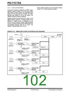
13.2.3 READING THE CAPTURE REGISTERS
An example of an instruction sequence to read capture
registers and capture overflow flag bits is shown in
Example 13-1. Depending on the capture source, dif-
ferent registers will need to be read.
The Capture overflow status flag bits are double
buffered. The master bit is set if one captured word is
already residing in the Capture register and another
“event” has occurred on the CAPx pin. The new event
will not transfer the TMR3 value to the capture register,
protecting the previous unread capture value. When
the user reads both the high and the low bytes (in any
order) of the Capture register, the master overflow bit is
transferred to the slave overflow bit (CAxOVF) and
then the master bit is reset. The user can then read
TCONx to determine the value of CAxOVF.
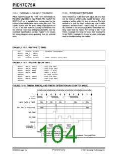
EXAMPLE 13-1: SEQUENCE TO READ CAPTURE REGISTERS
MOVLB 3
; Select Bank 3
MOVPF CA2L, LO_BYTE
MOVPF CA2H, HI_BYTE
MOVPF TCON2, STAT_VAL
; Read Capture2 low byte, store in LO_BYTE
; Read Capture2 high byte, store in HI_BYTE
; Read TCON2 into file STAT_VAL
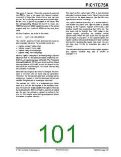
TABLE 13-6: REGISTERS ASSOCIATED WITH CAPTURE
Value on
POR,
BOR
Value on all
other resets
(Note1)
Address
Name
Bit 7
Bit 6
Bit 5
Bit 4
Bit 3
Bit 2
Bit 1
Bit 0
16h, Bank 3
17h, Bank 3
TCON1
TCON2
CA2ED1 CA2ED0 CA1ED1
CA1ED0
T16
TMR3CS TMR2CS TMR1CS 0000 0000 0000 0000
CA2OVF CA1OVF PWM2ON PWM1ON CA1/PR3 TMR3ON TMR2ON TMR1ON 0000 0000 0000 0000
CA4OVF CA3OVF CA4ED1 CA4ED0 CA3ED1 CA3ED0 PWM3ON -000 0000 -000 0000
16h, Bank 7
12h, Bank 2
13h, Bank 2
16h, Bank 1
17h, Bank 1
10h, Bank 4
11h, Bank 4
TCON3
TMR3L
TMR3H
PIR1
—
Holding register for the low byte of the 16-bit TMR3 register
Holding register for the high byte of the 16-bit TMR3 register
xxxx xxxx uuuu uuuu
xxxx xxxx uuuu uuuu
0000 0010 0000 0010
0000 0000 0000 0000
000- 0010 000- 0010
000- 0000 000- 0000
0000 0000 0000 0000
--11 1100 --11 qq11
xxxx xxxx uuuu uuuu
xxxx xxxx uuuu uuuu
xxxx xxxx uuuu uuuu
xxxx xxxx uuuu uuuu
xxxx xxxx uuuu uuuu
xxxx xxxx uuuu uuuu
xxxx xxxx uuuu uuuu
xxxx xxxx uuuu uuuu
RBIF
RBIE
SSPIF
SSPIE
PEIF
—
TMR3IF
TMR3IE
BCLIF
BCLIE
T0CKIF
—
TMR2IF
TMR2IE
ADIF
TMR1IF
TMR1IE
—
CA2IF
CA2IE
CA4IF
CA4IE
PEIE
CA1IF
CA1IE
CA3IF
CA3IE
T0CKIE
PD
TX1IF
TX1IE
TX2IF
TX2IE
T0IE
RC1IF
RC1IE
RC2IF
RC2IE
INTE
PIE1
PIR2
PIE2
ADIE
—
07h, Unbanked INTSTA
06h, Unbanked CPUSTA
T0IF
INTF
STKAV
GLINTD
TO
POR
BOR
16h, Bank 2
17h, Bank 2
14h, Bank 3
15h, Bank 3
12h, Bank 7
13h, Bank 7
14h, Bank 7
15h, Bank 7
Legend:
PR3L/CA1L Timer3 period register, low byte/capture1 register, low byte
PR3H/CA1H Timer3 period register, high byte/capture1 register, high byte
CA2L
CA2H
CA3L
CA3H
CA4L
CA4H
Capture2 low byte
Capture2 high byte
Capture3 low byte
Capture3 high byte
Capture4 low byte
Capture4 high byte
x= unknown, u= unchanged, -= unimplemented read as '0', q- value depends on condition,
shaded cells are not used by Capture.
Note 1:
Other (non power-up) resets include: external reset through MCLR and WDT Timer Reset.
1997 Microchip Technology Inc.
Preliminary
DS30264A-page 103

 MICROCHIP [ MICROCHIP ]