PIC17C75X
13.1.3 USING PULSE WIDTH MODULATION
(PWM) OUTPUTS WITH TIMER1 AND
TIMER2
The user needs to set the PWM1ON bit (TCON2<4>)
to enable the PWM1 output. When the PWM1ON bit is
set, the RB2/PWM1 pin is configured as PWM1 output
and forced as an output irrespective of the data direc-
tion bit (DDRB<2>). When the PWM1ON bit is clear,
the pin behaves as a port pin and its direction is con-
trolled by its data direction bit (DDRB<2>). Similarly,
the PWM2ON (TCON2<5>) bit controls the configura-
tion of the RB3/PWM2 pin and the PWM3ON
(TCON3<0>) bit controls the configuration of the
RG5/PWM3 pin.
Three high speed pulse width modulation (PWM) out-
puts are provided. The PWM1 output uses Timer1 as
its time-base, while PWM2 and PWM3 may indepen-
dently be software configured to use either Timer1 or
Timer2 as the time-base. The PWM outputs are on the
RB2/PWM1, RB3/PWM2, and RG5/PWM3 pins.
Each PWM output has a maximum resolution of
10-bits. At 10-bit resolution, the PWM output frequency
is 32.2 kHz (@ 32 MHz clock) and at 8-bit resolution the
PWM output frequency is 128.9 kHz. The duty cycle of
the output can vary from 0% to 100%.
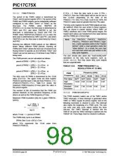
FIGURE 13-6: SIMPLIFIED PWM BLOCK
DIAGRAM
PWxDCL<7:6>
Write
Duty Cycle registers
PWxDCH
Figure 13-6 shows a simplified block diagram of a
PWM module.
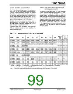
The duty cycle registers are double buffered for glitch
free operation. Figure 13-7 shows how a glitch could
occur if the duty cycle registers were not double buff-
ered.
Read
(Slave)
PWMx
Comparator
R
S
Q
TMRx
(Note 1)
PWMxON
Comparator
Clear Timer,
PWMx pin and
Latch D.C.
PRy
Note 1: 8-bit timer is concatenated with 2-bit internal Q clock
or 2 bits of the prescaler to create 10-bit time-base.
FIGURE 13-7: PWM OUTPUT
0
10
20
30
40
0
PWM
output
Timer
interrupt
Write new
PWM value
Timer interrupt
new PWM value
transferred to slave
Note The dotted line shows PWM output if duty cycle registers were not double buffered.
If the new duty cycle is written after the timer has passed that value, then the PWM does
not reset at all during the current cycle causing a “glitch”.
In this example, PWM period = 50. Old duty cycle is 30. New duty cycle value is 10.
1997 Microchip Technology Inc.
Preliminary
DS30264A-page 97

 MICROCHIP [ MICROCHIP ]