PIC17C75X
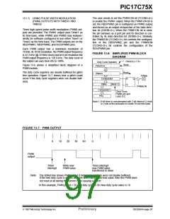
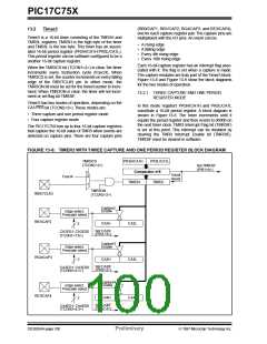
This mode (3 Capture, 1 Period) is selected if control bit
CA1/PR3 is clear. In this mode, the Capture1 register,
consisting of high byte (PR3H/CA1H) and low byte
(PR3L/CA1L), is configured as the period control regis-
ter for TMR3. Capture1 is disabled in this mode, and
the corresponding Interrupt bit CA1IF is never set.
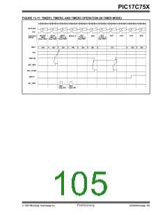
TMR3 increments until it equals the value in the period
register and then resets to 0000h on the next timer
clock.
The input on the capture pin CAPx is synchronized
internally to internal phase clocks.This imposes certain
restrictions on the input waveform (see the Electrical
Specification section for timing).
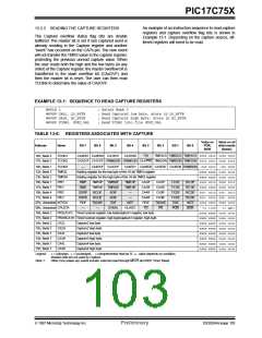
The capture overflow status flag bit is double buffered.
The master bit is set if one captured word is already
residing in the Capture register (CAxH:CAxL) and
another “event” has occurred on the CAPx pin. The
new event will not transfer the TMR3 value to the
capture register, protecting the previous unread
capture value. When the user reads both the high and
the low bytes (in any order) of the Capture register, the
master overflow bit is transferred to the slave overflow
bit (CAxOVF) and then the master bit is reset.The user
can then read TCONx to determine the value of
CAxOVF.
All other Captures are active in this mode.
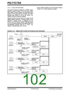
13.2.1.1 CAPTURE OPERATION
The CAxED1 and CAxED0 bits determine the event on
which capture will occur. The possible events are:
• Capture on every falling edge
• Capture on every rising edge
• Capture every 4th rising edge
• Capture every 16th rising edge
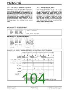
The recommended sequence to read capture registers
and capture overflow flag bits is shown in
Example 13-1.
When a capture takes place, an interrupt flag is latched
into the CAxIF bit.This interrupt can be enabled by set-
ting the corresponding mask bit CAxIE. The Peripheral
Interrupt Enable bit (PEIE) must be set and the Global
Interrupt Disable bit (GLINTD) must be cleared for the
interrupt to be acknowledged. The CAxIF interrupt flag
bit is cleared in software.
When the capture prescale select is changed, the pres-
caler is not reset and an event may be generated.
Therefore, the first capture after such a change will be
ambiguous. However, it sets the time-base for the next
capture. The prescaler is reset upon chip reset.
The capture pin, CAPx, is a multiplexed pin. When
used as a port pin, the capture is not disabled. How-
ever, the user can simply disable the Capture interrupt
by clearing CAxIE. If the CAPx pin is used as an output
pin, the user can activate a capture by writing to the
port pin.This may be useful during development phase
to emulate a capture interrupt.
1997 Microchip Technology Inc.
Preliminary
DS30264A-page 101

 MICROCHIP [ MICROCHIP ]