PIC17C75X
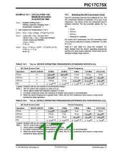
EXAMPLE 16-1: CALCULATING THE
MINIMUM REQUIRED
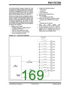
16.2
Selecting the A/D Conversion Clock
The A/D conversion time per bit is defined as TAD. The
A/D conversion requires a minimum 12TAD per 10-bit
conversion. The source of the A/D conversion clock is
software selected. The four possible options for TAD
are:
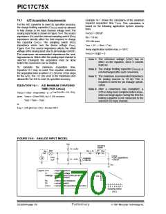
ACQUISITION TIME
TACQ = Amplifier Settling Time +
Holding Capacitor Charging Time +
Temperature Coefficient †
• 8TOSC
† Only required for temperatures ≠ 25°C
TACQ = 10 µs + Tcap + [(Temp - 25°C)(0.05 µs/°C)]
• 32TOSC
• 64TOSC
TCAP = -CHOLD (RIC + RSS + RS) ln(1/2047)
-200 pF (1 kΩ + 7 kΩ + 10 kΩ) ln(0.0004885)
-200 pF (18 kΩ) ln(0.0004885)
-3.6 µs (-7.6241)
• Internal RC oscillator
For correct A/D conversions, the A/D conversion clock
(TAD) must be selected to ensure a minimum TAD time
of 1.6 µs.
27.447 µs
Table 16-1 and Table 16-2 show the resultant TAD
times derived from the device operating frequencies
and the A/D clock source selected. These times are for
standard voltage range devices.
TACQ = 10 µs + 27.447 µs + [(50°C - 25°C)(0.05 µs/°C)]
37.447 µs + 1.25 µs
38.697 µs
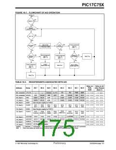
TABLE 16-1: TAD vs. DEVICE OPERATING FREQUENCIES (STANDARD DEVICES (C))
AD Clock Source (TAD)
Operation ADCS1:ADCS0
Device Frequency
33 MHz
20 MHz
5 MHz
1.6 µs
6.4 µs
1.25 MHz
333.33 kHz
(2)
(2)
8TOSC
32TOSC
64TOSC
RC
00
01
10
11
6.4 µs
24 µs
242 ns
970 ns
400 ns
(2)
(3)
(3)
1.6 µs
25.6 µs
96 µs
(3)
(3)
(3)
1.94 µs
3.2 µs
12.8 µs
51.2 µs
192 µs
(1, 4)
(1, 4)
(1, 4)
(1, 4)
(1)
2 - 6 µs
2 - 6 µs
2 - 6 µs
2 - 6 µs
2 - 6 µs
Legend: Shaded cells are are outside of recommended ranges.
Note 1: The RC source has a typical TAD time of 4 µs.
2: These values violate the minimum required TAD time.
3: For faster conversion times, the selection of another clock source is recommended.
4: When the device frequencies is greater than 1 MHz, the RC A/D conversion clock source is only recom-
mended for sleep operation.
TABLE 16-2: TAD vs. DEVICE OPERATING FREQUENCIES (EXTENDED VOLTAGE DEVICES (LC))
AD Clock Source (TAD)
Operation ADCS1:ADCS0
Device Frequency
8 MHz
4 MHz
2 MHz
4 µs
1 MHz
333.33 kHz
(2)
(2)
8TOSC
32TOSC
64TOSC
RC
00
01
10
11
8 µs
24 µs
1.0 µs
4.0 µs
2.0 µs
8 µs
(3)
(3)
16 µs
32 µs
64 µs
96 µs
(3)
(3)
(1)
(3)
8.0 µs
16 µs
32 µs
192 µs
(1, 4)
(1, 4)
(1, 4)
(1)
3 - 9 µs
3 - 9 µs
3 - 9 µs
3 - 9 µs
3 - 9 µs
Legend: Shaded cells are are outside of recommended ranges.
Note 1: The RC source has a typical TAD time of 4 µs.
2: These values violate the minimum required TAD time.
3: For faster conversion times, the selection of another clock source is recommended.
4: When the device frequencies is greater than 1 MHz, the RC A/D conversion clock source is only recom-
mended for sleep operation.
1997 Microchip Technology Inc.
Preliminary
DS30264A-page 171

 MICROCHIP [ MICROCHIP ]