PIC17C75X
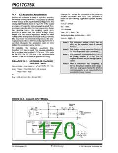
Example 16-1 shows the calculation of the minimum
required acquisition time TACQ. This calculation is
based on the following application system assump-
tions.
16.1
A/D Acquisition Requirements
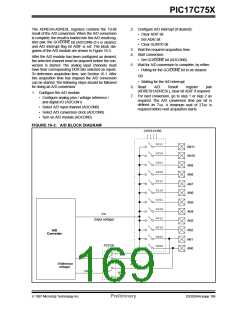
For the A/D converter to meet its specified accuracy,
the charge holding capacitor (CHOLD) must be allowed
to fully charge to the input channel voltage level. The
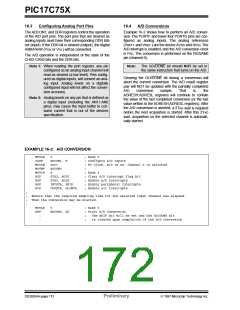
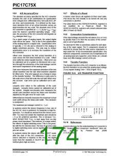
analog input model is shown in Figure 16-4.The source
impedance (RS) and the internal sampling switch (RSS)
impedance directly affect the time required to charge
the capacitor CHOLD. The sampling switch (RSS)
impedance varies over the device voltage (VDD),
Figure 16-4. The source impedance affects the offset
voltage at the analog input (due to pin leakage current).
The maximum recommended impedance for ana-
log sources is 10 kΩ. After the analog input channel is
selected (changed) this acquisition must be done
before the conversion can be started.
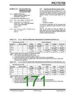
CHOLD = 200 pF
Rs = 10 kΩ
1/2 LSb error
VDD = 5V → Rss = 7 kΩ
Temp (application system max.) = 50°C
VHOLD = 0 @ t = 0
Note 1: The reference voltage (VREF) has no
effect on the equation, since it cancels
itself out.
To calculate the minimum acquisition time,
Equation 16-1 may be used. This equation calculates
the acquisition time to within 1/2 LSb error (1024 steps
for the A/D). The 1/2 LSb error is the maximum error
allowed for the A/D to meet its specified accuracy.
Note 2: The charge holding capacitor (CHOLD) is
not discharged after each conversion.
Note 3: The maximum recommended impedance
for analog sources is 10 kΩ. This is
required to meet the pin leakage specifi-
cation.
EQUATION 16-1: A/D MINIMUM CHARGING
TIME (FOR CHOLD)
Note 4: After a conversion has completed, a
2.0TAD delay must complete before acqui-
sition can begin again. During this time the
holding capacitor is not connected to the
selected A/D input channel.
(-Tcap/CHOLD(RIC + RSS + RS))
VHOLD = (VREF - (VREF/2048)) • (1 - e
given VHOLD = (VREF/2048), for 1/2 LSb resolution
VREF = VREF+ - VREF-
)
or
Tcap = -(200 pF)(1 kΩ + RSS + RS) ln(1/2047)
FIGURE 16-4: ANALOG INPUT MODEL
VDD
Sampling
Switch
VT = 0.6V
VT = 0.6V
ANx
SS
RIC ≤ 1k
RSS
Rs
CHOLD
= DAC capacitance
= 200 pF
CPIN
5 pF
VA
I leakage
± 500 nA
VSS
Legend CPIN
VT
= input capacitance
= threshold voltage
6V
5V
I leakage = leakage current at the pin due to
various junctions
VDD 4V
3V
2V
RIC
SS
= interconnect resistance
= sampling switch
CHOLD
= sample/hold capacitance (from DAC)
5 6 7 8 9 10 11
Sampling Switch
( kΩ )
DS30264A-page 170
Preliminary
1997 Microchip Technology Inc.

 MICROCHIP [ MICROCHIP ]