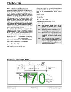
PIC17C75X
16.6
A/D Accuracy/Error
16.7
Effects of a Reset
The absolute accuracy specified for the A/D converter
includes the sum of all contributions for quantization
error, integral error, differential error, full scale error, off-
set error, and monotonicity. It is defined as the maxi-
mum deviation from of an actual transition versus an
ideal transition for any code. The absolute error of the
A device reset forces all registers to their reset state.
This forces the A/D module to be turned off, and any
conversion is aborted.
The value that is in the ADRESH:ADRESL registers is
not modified for
a
Power-on Reset. The
ADRESH:ADRESL registers will contain unknown data
after a Power-on Reset.
A/D converter is specified at < + 1 LSb for V = V
DD
REF
(over the device’s specified operating range). How-
ever, the accuracy of the A/D converter will degrade as
16.8
Connection Considerations
V
diverges from V
.
DD
REF
If the input voltage exceeds the rail values (VSS or VDD)
by greater than 0.3V, then the accuracy of the conver-
sion is out of specification.
For a given range of analog inputs, the output digital
code will be the same. This is due to the quantization
of the analog input to a digital code. Quantization error
is typically + 1/2 LSb and is inherent in the analog to
digital conversion process. The only way to reduce
quantization error is to increase the resolution of the
A/D converter.
An external RC filter is sometimes added for anti-alias-
ing of the input signal. The R component should be
selected to ensure that the total source impedance is
kept under the 10 kΩ recommended specification. Any
external components connected (via hi-impedance) to
an analog input pin (capacitor, zener diode, etc.) should
have very little leakage current at the pin.
Offset error measures the first actual transition of a
code versus the first ideal transition of a code. Offset
error shifts the entire transfer function. Offset error can
be calibrated out of a system or introduced into a sys-
tem through the interaction of the total leakage current
and source impedance at the analog input.
16.9
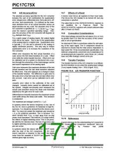
Transfer Function
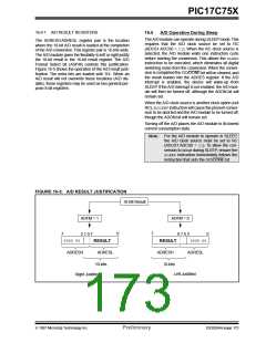
The transfer function of the A/D converter is as follows:
the first transition occurs when the analog input voltage
(VAIN) equals Analog VREF / 1024 (Figure 16-6).
Gain error measures the maximum deviation of the last
actual transition and the last ideal transition adjusted
for offset error. This error appears as a change in slope
of the transfer function. The difference is gain error to
full scale error is that full scale doe not take offset error
into account. Gain error can be calibrated out in soft-
ware.
FIGURE 16-6: A/D TRANSFER FUNCTION
3FFh
3FEh
Linearity error refers to the uniformity of the code
changes. Linearity errors cannot be calibrated out of
the system. Integral non-linearity error measures the
actual code transition versus the ideal code transition
adjusted by the gain error for each code.
003h
002h
001h
000h
Differential non-linearity measures the maximum actual
code width versus the ideal code width. This measure
is unadjusted.
The maximum pin leakage current is ± 1 µA.
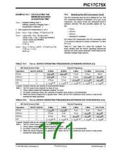
In systems where the device frequency is low, use of
the A/D RC clock is preferred. At moderate to high fre-
quencies, TAD should be derived from the device oscil-
lator. TAD must not violate the minimum and should be
≤ 8 µs for preferred operation. This is because TAD,
when derived from TOSC, is kept away from on-chip
phase clock transitions.This reduces, to a large extent,
the effects of digital switching noise. This is not possi-
ble with the RC derived clock.The loss of accuracy due
to digital switching noise can be significant if many I/O
pins are active.
Analog input voltage
16.10 References
A good reference for the undestanding A/D converter is
the "Analog-Digital Conversion Handbook" third edi-
tion,
published
by
Prentice
Hall
(ISBN
0-13-03-2848-0).
In systems where the device will enter SLEEP mode
after the start of the A/D conversion, the RC clock
source selection is required. In this mode, the digital
noise from the modules in SLEEP are stopped. This
method gives high accuracy.
DS30264A-page 174
Preliminary
1997 Microchip Technology Inc.

 MICROCHIP [ MICROCHIP ]