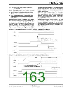
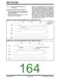
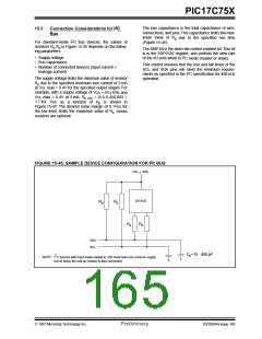
PIC17C75X
The A/D module has four registers. These registers
are:
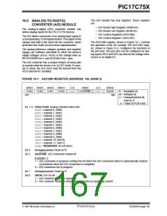
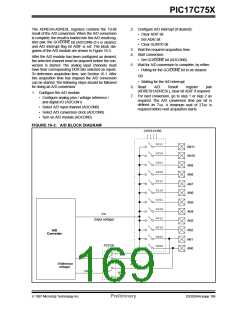
16.0 ANALOG-TO-DIGITAL
CONVERTER (A/D) MODULE
The analog-to-digital (A/D) converter module has
twelve analog inputs for the PIC17C75X devices.
• A/D Result High Register (ADRESH)
• A/D Result Low Register (ADRESL)
• A/D Control Register0 (ADCON0)
• A/D Control Register1 (ADCON1)
The A/D allows conversion of an analog input signal to
a corresponding 10-bit digital number.The output of the
sample and hold is the input into the converter, which
generates the result via successive approximation.
The ADCON0 register, shown in Figure 16-1, controls
the operation of the A/D module. The ADCON1 regis-
ter, shown in Figure 16-2, configures the functions of
the port pins. The port pins can be configured as ana-
log inputs (RG3 and RG2 can also be the voltage refer-
ences) or as digital I/O.
The analog reference voltages (positive and negative
supply) are software selectable to either the device’s
supply voltages (AVDD, AVss) or the voltage level on
the RG3/AN0/VREF+ and RG2/AN1/VREF- pins.
The A/D converter has a unique feature of being able
to operate while the device is in SLEEP mode.To oper-
ate in sleep, the A/D clock must be derived from the
A/D’s internal RC oscillator.
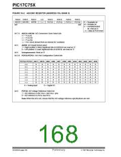
FIGURE 16-1: ADCON0 REGISTER (ADDRESS: 14h, BANK 5)
R/W-0 R/W-0 R/W-0
CHS3 CHS2 CHS1
bit7
R/W-0
CHS0
U-0
—
R/W-0
U-0
—
R/W-0
ADON
GO/DONE
R =Readable bit
W = Writable bit
U =Unimplemented bit,
read as ‘0’
bit0
- n = Value at POR reset
bit 7-4: CHS2:CHS0: Analog Channel Select bits
0000= channel 0, (AN0)
0001= channel 1, (AN1)
0010= channel 2, (AN2)
0011= channel 3, (AN3)
0100= channel 4, (AN4)
0101= channel 5, (AN5)
0110= channel 6, (AN6)
0111= channel 7, (AN7)
1000= channel 8, (AN8)
1001= channel 9, (AN9)
1010= channel 10, (AN10)
1011= channel 11, (AN11)
11xx= RESERVED, do not select
bit 3:
bit 2:
Unimplemented: Read as '0'
GO/DONE: A/D Conversion Status bit
If ADON = 1
1 = A/D conversion in progress (setting this bit starts the A/D conversion which is automatically cleared
by hardware when the A/D conversion is complete)
0 = A/D conversion not in progress
bit 1:
bit 0:
Unimplemented: Read as '0'
ADON: A/D On bit
1 = A/D converter module is operating
0 = A/D converter module is shutoff and consumes no operating current
1997 Microchip Technology Inc.
Preliminary
DS30264A-page 167

 MICROCHIP [ MICROCHIP ]