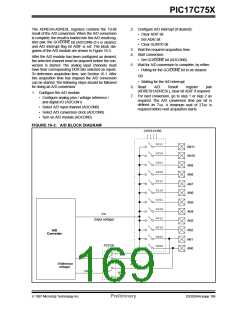
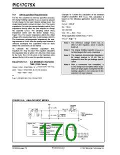
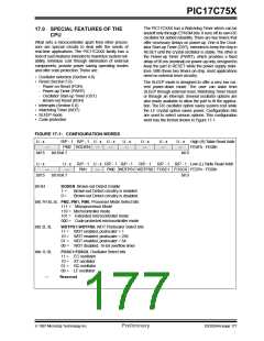
PIC17C75X
16.4.1 A/D RESULT REGISTERS
16.5
A/D Operation During Sleep
The A/D module can operate during SLEEP mode.This
requires that the A/D clock source be set to RC
(ADCS1:ADCS0 = 11). When the RC clock source is
selected, the A/D module waits one instruction cycle
before starting the conversion. This allows the SLEEP
instruction to be executed, which eliminates all digital
switching noise from the conversion. When the conver-
sion is completed the GO/DONE bit will be cleared, and
the result loaded into the ADRES register. If the A/D
interrupt is enabled, the device will wake-up from
SLEEP. If the A/D interrupt is not enabled, the A/D mod-
ule will then be turned off, although the ADON bit will
remain set.
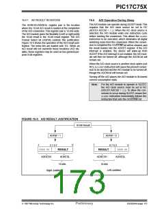
The ADRESH:ADRESL register pair is the location
where the 10-bit A/D result is loaded at the completion
of the A/D conversion.This register pair is 16-bits wide.
The A/D module gives the flexibility to left or right justify
the 10-bit result in the 16-bit result register. The A/D
Format Select bit (ADFM) controls this justification.
Figure 16-5 shows the operation of the A/D result justi-
fication. The extra bits are loaded with ’0’s’. When an
A/D result will not overwrite these locations (A/D dis-
able), these registers may be used as two general pur-
pose 8-bit registers.
When the A/D clock source is another clock option (not
RC), a SLEEPinstruction will cause the present conver-
sion to be aborted and the A/D module to be turned off,
though the ADON bit will remain set.
Turning off the A/D places the A/D module in its lowest
current consumption state.
Note: For the A/D module to operate in SLEEP,
the A/D clock source must be set to RC
(ADCS1:ADCS0 = 11). To allow the con-
version to occur during SLEEP, ensure the
SLEEPinstruction immediately follows the
instruction that sets the GO/DONE bit.
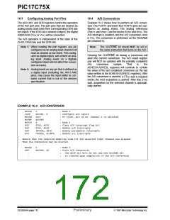
FIGURE 16-5: A/D RESULT JUSTIFICATION
10-Bit Result
ADFM = 1
2 1 0 7
ADFM = 0
0
7
7
0 7 6 5
0
0000 00
0000 00
RESULT
ADRESL
10-bits
RESULT
ADRESH
10-bits
ADRESH
ADRESL
Left Justified
Right Justified
1997 Microchip Technology Inc.
Preliminary
DS30264A-page 173

 MICROCHIP [ MICROCHIP ]