PIC17C75X
16.3
Configuring Analog Port Pins
16.4
A/D Conversions
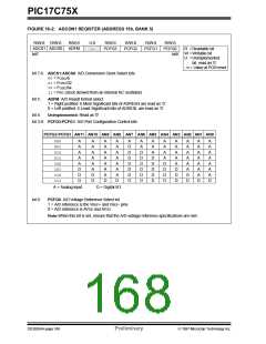
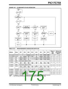
The ADCON1, and DDR registers control the operation
of the A/D port pins. The port pins that are desired as
analog inputs must have their corresponding DDR bits
set (input). If the DDR bit is cleared (output), the digital
output level (VOH or VOL) will be converted.
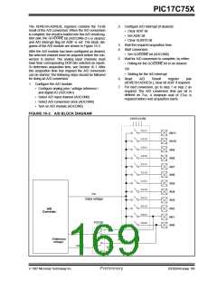
Example 16-2 shows how to perform an A/D conver-
sion. The PORTF and lower four PORTG pins are con-
figured as analog inputs. The analog references
(VREF+ and VREF-) are the device AVDD and AVSS.The
A/D interrupt is enabled, and the A/D conversion clock
is FRC. The conversion is performed on the RG3/AN0
pin (channel 0).
The A/D operation is independent of the state of the
CHS2:CHS0 bits and the DDR bits.
Note 1: When reading the port register, any pin
configured as an analog input channel will
read as cleared (a low level). Pins config-
ured as digital inputs, will convert an ana-
log input. Analog levels on a digitally
configured input will not affect the conver-
sion accuracy.
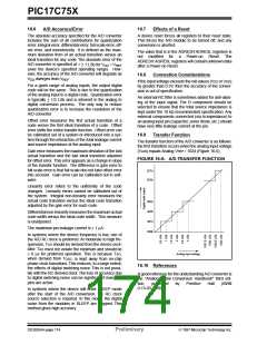
Note: The GO/DONE bit should NOT be set in
the same instruction that turns on the A/D.
Clearing the GO/DONE bit during a conversion will
abort the current conversion. The A/D result register
pair will NOT be updated with the partially completed
A/D
conversion
sample.
That
is,
the
ADRESH:ADRESL registers will continue to contain
the value of the last completed conversion (or the last
value written to the ADRESH:ADRESL registers). After
the A/D conversion is aborted, a 2TAD wait is required
before the next acquisition is started. After this 2TAD
wait, acquisition on the selected channel is automati-
cally started.
Note 2: Analog levels on any pin that is defined as
a digital input (including the AN11:AN0
pins), may cause the input buffer to con-
sume current that is out of the devices
specification.
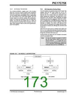
EXAMPLE 16-2: A/D CONVERSION
MOVLB
CLRF
MOVLW
MOVWF
MOVLB
BCF
BSF
BSF
BCF
5
; Bank 5
ADCON1, F
0xC1
ADCON0
; Configure A/D inputs
; RC Clock, A/D is on, Channel 0 is selected
;
4
; Bank 4
PIR2, ADIF
PIE2, ADIE
INTSTA, PEIE
CPUSTA, GLINTD
; Clear A/D interrupt flag bit
; Enable A/D interrupts
; Enable peripheral interrupts
; Enable all interrupts
;
;
;
;
Ensure that the required sampling time for the selected input channel has elapsed.
Then the conversion may be started.
MOVLB
5
; Bank 5
BSF
:
:
ADCON0, GO
; Start A/D Conversion
;
;
The ADIF bit will be set and the GO/DONE bit
is cleared upon completion of the A/D Conversion
DS30264A-page 172
Preliminary
1997 Microchip Technology Inc.

 MICROCHIP [ MICROCHIP ]