PIC17C75X
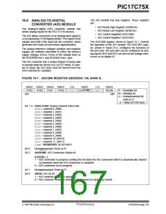
The ADRESH:ADRESL registers contains the 10-bit
result of the A/D conversion. When the A/D conversion
is complete, the result is loaded into this A/D result reg-
ister pair, the GO/DONE bit (ADCON0<2>) is cleared,
and A/D interrupt flag bit ADIF is set. The block dia-
grams of the A/D module are shown in Figure 16-3.
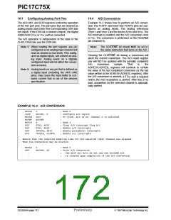
2. Configure A/D interrupt (if desired):
• Clear ADIF bit
• Set ADIE bit
• Clear GLINTD bit
3. Wait the required acquisition time.
4. Start conversion:
After the A/D module has been configured as desired,
the selected channel must be acquired before the con-
version is started. The analog input channels must
have their corresponding DDR bits selected as inputs.
To determine acquisition time, see Section 16.1. After
this acquisition time has elapsed the A/D conversion
can be started. The following steps should be followed
for doing an A/D conversion:
• Set GO/DONE bit (ADCON0)
5. Wait for A/D conversion to complete, by either:
• Polling for the GO/DONE bit to be cleared
OR
• Waiting for the A/D interrupt
6. Read
A/D
Result
register
pair
(ADRESH:ADRESL), clear bit ADIF if required.
1. Configure the A/D module:
7. For next conversion, go to step 1 or step 2 as
required. The A/D conversion time per bit is
defined as TAD. A minimum wait of 2TAD is
required before next acquisition starts.
• Configure analog pins / voltage reference /
and digital I/O (ADCON1)
• Select A/D input channel (ADCON0)
• Select A/D conversion clock (ADCON0)
• Turn on A/D module (ADCON0)
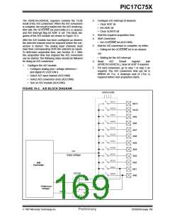
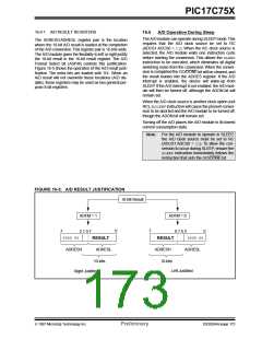
FIGURE 16-3: A/D BLOCK DIAGRAM
CHS3:CHS0
1011
AN11
1010
AN10
1001
AN9
1000
AN8
0111
AN7
0110
AN6
0101
AN5
0100
AN4
VIN
0011
(Input voltage)
AN3
0010
AN2
A/D
Converter
0001
AN1
PCFG0
0000
AN0
VREF-
(Reference
voltage)
AVSS
VREF+
AVDD
1997 Microchip Technology Inc.
Preliminary
DS30264A-page 169

 MICROCHIP [ MICROCHIP ]