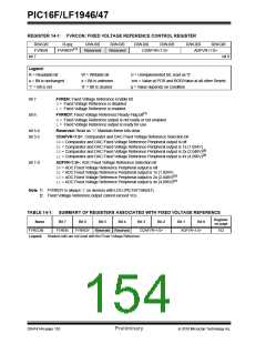
PIC16F/LF1946/47
15.1.5
INTERRUPTS
15.1.6
RESULT FORMATTING
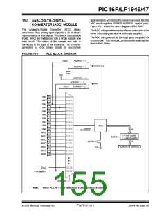
The ADC module allows for the ability to generate an
interrupt upon completion of an Analog-to-Digital
conversion. The ADC Interrupt Flag is the ADIF bit in
the PIR1 register. The ADC Interrupt Enable is the
ADIE bit in the PIE1 register. The ADIF bit must be
cleared in software.
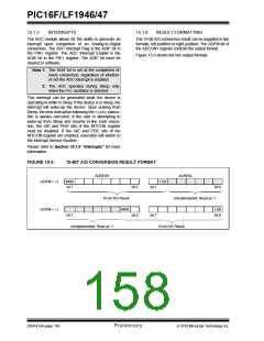
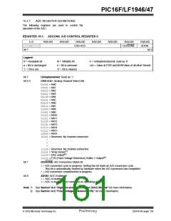
The 10-bit A/D conversion result can be supplied in two
formats, left justified or right justified. The ADFM bit of
the ADCON1 register controls the output format.
Figure 15-3 shows the two output formats.
Note 1: The ADIF bit is set at the completion of
every conversion, regardless of whether
or not the ADC interrupt is enabled.
2: The ADC operates during Sleep only
when the FRC oscillator is selected.
This interrupt can be generated while the device is
operating or while in Sleep. If the device is in Sleep, the
interrupt will wake-up the device. Upon waking from
Sleep, the next instruction following the SLEEPinstruc-
tion is always executed. If the user is attempting to
wake-up from Sleep and resume in-line code execu-
tion, the GIE and PEIE bits of the INTCON register
must be disabled. If the GIE and PEIE bits of the
INTCON register are enabled, execution will switch to
the Interrupt Service Routine.
Please refer to Section 15.1.5 “Interrupts” for more
information.
FIGURE 15-3:
10-BIT A/D CONVERSION RESULT FORMAT
ADRESH
ADRESL
LSB
(ADFM = 0)
MSB
bit 7
bit 0
bit 0
bit 7
bit 7
bit 0
10-bit A/D Result
Unimplemented: Read as ‘0’
(ADFM = 1)
MSB
LSB
bit 0
bit 7
Unimplemented: Read as ‘0’
10-bit A/D Result
DS41414A-page 156
Preliminary
2010 Microchip Technology Inc.

 MICROCHIP [ MICROCHIP ]