PIC16F/LF1946/47
approximation and stores the conversion result into the
ADC result registers (ADRESH:ADRESL register pair).
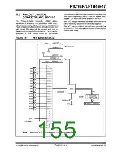
Figure 15-1 shows the block diagram of the ADC.
15.0 ANALOG-TO-DIGITAL
CONVERTER (ADC) MODULE
The Analog-to-Digital Converter (ADC) allows
conversion of an analog input signal to a 10-bit binary
representation of that signal. This device uses analog
inputs, which are multiplexed into a single sample and
hold circuit. The output of the sample and hold is
connected to the input of the converter. The converter
generates a 10-bit binary result via successive
The ADC voltage reference is software selectable to be
either internally generated or externally supplied.
The ADC can generate an interrupt upon completion of
a conversion. This interrupt can be used to wake-up the
device from Sleep.
FIGURE 15-1:
ADC BLOCK DIAGRAM
ADNREF = 1
VREF-
ADNREF = 0
VSS
VDD
ADPREF = 00
ADPREF = 11
VREF+
ADPREF = 10
AN0
AN1
00000
00001
00010
00011
00100
00101
AN2
AN3
AN4
AN5
AN6
00110
00111
01000
01001
01010
01011
01100
01101
01110
01111
10000
AN7
AN8
ADC
AN9
10
GO/DONE
AN10
AN11
AN12
AN13
AN14
AN15
AN16
0= Left Justify
ADFM
1= Right Justify
ADON
16
ADRESH ADRESL
VSS
11110
11111
DAC
FVR Buffer1
CHS<4:0>
Note:
When ADON = 0, all multiplexer inputs are disconnected.
2010 Microchip Technology Inc.
Preliminary
DS41414A-page 153

 MICROCHIP [ MICROCHIP ]