PIC16F/LF1946/47
15.1.4
CONVERSION CLOCK
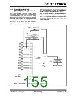
15.1 ADC Configuration
The source of the conversion clock is software select-
able via the ADCS bits of the ADCON1 register. There
are seven possible clock options:
When configuring and using the ADC the following
functions must be considered:
• Port configuration
• FOSC/2
• Channel selection
• FOSC/4
• ADC voltage reference selection
• ADC conversion clock source
• Interrupt control
• FOSC/8
• FOSC/16
• FOSC/32
• Result formatting
• FOSC/64
15.1.1
PORT CONFIGURATION
• FRC (dedicated internal oscillator)
The ADC can be used to convert both analog and
digital signals. When converting analog signals, the I/O
pin should be configured for analog by setting the
associated TRIS and ANSEL bits. Refer to
Section 12.0 “I/O Ports” for more information.
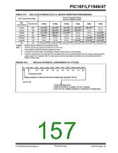
The time to complete one bit conversion is defined as
TAD. One full 10-bit conversion requires 11.5 TAD
periods as shown in Figure 15-2.
For correct conversion, the appropriate TAD specifica-
tion must be met. Refer to the A/D conversion require-
ments in Section 29.0 “Electrical Specifications” for
more information. Table 15-1 gives examples of
appropriate ADC clock selections.
Note:
Analog voltages on any pin that is defined
as a digital input may cause the input buf-
fer to conduct excess current.
Note:
Unless using the FRC, any changes in the
system clock frequency will change the
ADC clock frequency, which may
adversely affect the ADC result.
15.1.2
CHANNEL SELECTION
There are 16 channel selections available:
• AN<13:0> pins
• DAC Output
• FVR (Fixed Voltage Reference) Output
Refer to Section 16.0 “Digital-to-Analog Converter
(DAC) Module” and Section 14.0 “Fixed Voltage
Reference (FVR)” for more information on these chan-
nel selections.
The CHS bits of the ADCON0 register determine which
channel is connected to the sample and hold circuit.
When changing channels, a delay is required before
starting the next conversion. Refer to Section 15.2
“ADC Operation” for more information.
15.1.3
ADC VOLTAGE REFERENCE
The ADPREF bits of the ADCON1 register provides
control of the positive voltage reference. The positive
voltage reference can be:
• VREF+ pin
• VDD
• FVR
The ADNREF bit of the ADCON1 register provides
control of the negative voltage reference. The negative
voltage reference can be:
• VREF- pin
• VSS
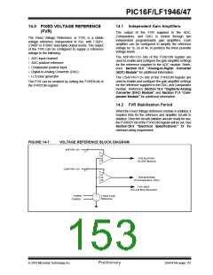
See Section 14.0 “Fixed Voltage Reference (FVR)”
for more details on the fixed voltage reference.
DS41414A-page 154
Preliminary
2010 Microchip Technology Inc.

 MICROCHIP [ MICROCHIP ]