PIC16F/LF1946/47
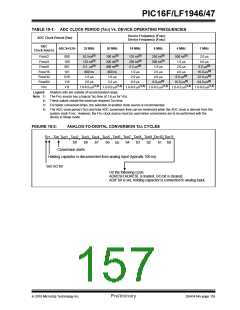
TABLE 15-1: ADC CLOCK PERIOD (TAD) VS. DEVICE OPERATING FREQUENCIES
Device Frequency (FOSC)
Device Frequency (FOSC)
ADC Clock Period (TAD)
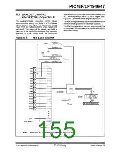
ADC
ADCS<2:0>
Clock Source
32 MHz
20 MHz
16 MHz
8 MHz
4 MHz
1 MHz
(2)
(2)
(2)
(2)
(2)
Fosc/2
Fosc/4
Fosc/8
Fosc/16
Fosc/32
Fosc/64
FRC
000
100
001
101
010
110
x11
62.5ns
125 ns
0.5 s
100 ns
200 ns
400 ns
125 ns
250 ns
250 ns
500 ns
500 ns
1.0 s
2.0 s
4.0 s
2.0 s
4.0 s
(2)
(2)
(2)
(2)
(2)
(2)
(2)
(3)
0.5 s
1.0 s
2.0 s
4.0 s
8.0 s
16.0 s
32.0 s
64.0 s
(3)
(3)
(3)
800 ns
1.0 s
800 ns
1.6 s
1.0 s
2.0 s
(3)
8.0 s
(3)
(3)
2.0 s
3.2 s
4.0 s
8.0 s
16.0 s
(1,4)
(1,4)
(1,4)
(1,4)
(1,4)
(1,4)
1.0-6.0 s
1.0-6.0 s
1.0-6.0 s
1.0-6.0 s
1.0-6.0 s
1.0-6.0 s
Legend:
Shaded cells are outside of recommended range.
Note 1: The FRC source has a typical TAD time of 1.6 s for VDD.
2: These values violate the minimum required TAD time.
3: For faster conversion times, the selection of another clock source is recommended.
4: The ADC clock period (TAD) and total ADC conversion time can be minimized when the ADC clock is derived from the
system clock FOSC. However, the FRC clock source must be used when conversions are to be performed with the
device in Sleep mode.
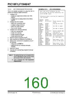
FIGURE 15-2:
ANALOG-TO-DIGITAL CONVERSION TAD CYCLES
TCY - TAD
TAD6 TAD7 TAD8 TAD9 TAD10 TAD11
TAD1 TAD2 TAD3 TAD4 TAD5
b7
b6
b4
b1
b0
b9
b8
b5
b3
b2
Conversion starts
Holding capacitor is disconnected from analog input (typically 100 ns)
Set GO bit
On the following cycle:
ADRESH:ADRESL is loaded, GO bit is cleared,
ADIF bit is set, holding capacitor is connected to analog input.
2010 Microchip Technology Inc.
Preliminary
DS41414A-page 155

 MICROCHIP [ MICROCHIP ]