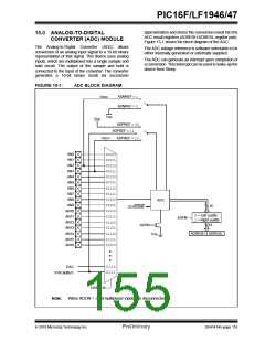
PIC16F/LF1946/47
15.2.4
ADC OPERATION DURING SLEEP
15.2 ADC Operation
The ADC module can operate during Sleep. This
requires the ADC clock source to be set to the FRC
option. When the FRC clock source is selected, the
ADC waits one additional instruction before starting the
conversion. This allows the SLEEP instruction to be
executed, which can reduce system noise during the
conversion. If the ADC interrupt is enabled, the device
will wake-up from Sleep when the conversion
completes. If the ADC interrupt is disabled, the ADC
module is turned off after the conversion completes,
although the ADON bit remains set.
15.2.1
STARTING A CONVERSION
To enable the ADC module, the ADON bit of the
ADCON0 register must be set to a ‘1’. Setting the GO/
DONE bit of the ADCON0 register to a ‘1’ will start the
Analog-to-Digital conversion.
Note:
The GO/DONE bit should not be set in the
same instruction that turns on the ADC.
Refer to Section 15.2.6 “A/D Conver-
sion Procedure”.
When the ADC clock source is something other than
FRC, a SLEEP instruction causes the present conver-
sion to be aborted and the ADC module is turned off,
although the ADON bit remains set.
15.2.2
COMPLETION OF A CONVERSION
When the conversion is complete, the ADC module will:
• Clear the GO/DONE bit
• Set the ADIF Interrupt Flag bit
15.2.5
SPECIAL EVENT TRIGGER
• Update the ADRESH and ADRESL registers with
new conversion result
The Special Event Trigger of the CCPx/ECCPX module
allows periodic ADC measurements without software
intervention. When this trigger occurs, the GO/DONE
bit is set by hardware and the Timer1 counter resets to
zero.
15.2.3
TERMINATING A CONVERSION
If a conversion must be terminated before completion,
the GO/DONE bit can be cleared in software. The
ADRESH and ADRESL registers will be updated with
the partially complete Analog-to-Digital conversion
sample. Incomplete bits will match the last bit
converted.
TABLE 15-2: SPECIAL EVENT TRIGGER
Device
CCPx/ECCPx
PIC16F/LF1946/47
CCP5
Using the Special Event Trigger does not assure proper
ADC timing. It is the user’s responsibility to ensure that
the ADC timing requirements are met.
Note:
A device Reset forces all registers to their
Reset state. Thus, the ADC module is
turned off and any pending conversion is
terminated.
Refer to Section 22.0 “Capture/Compare/PWM
Modules” for more information.
2010 Microchip Technology Inc.
Preliminary
DS41414A-page 157

 MICROCHIP [ MICROCHIP ]