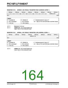
PIC16F/LF1946/47
15.2.6
A/D CONVERSION PROCEDURE
EXAMPLE 15-1:
A/D CONVERSION
This is an example procedure for using the ADC to
perform an Analog-to-Digital conversion:
;This code block configures the ADC
;for polling, Vdd and Vss references, Frc
;clock and AN0 input.
;
1. Configure Port:
• Disable pin output driver (Refer to the TRIS
register)
;Conversion start & polling for completion
; are included.
;
• Configure pin as analog (Refer to the ANSEL
register)
BANKSEL
MOVLW
ADCON1
;
B’11110000’ ;Right justify, Frc
;clock
2. Configure the ADC module:
• Select ADC conversion clock
• Configure voltage reference
• Select ADC input channel
• Turn on ADC module
MOVWF
BANKSEL
BSF
BANKSEL
BSF
BANKSEL
MOVLW
MOVWF
CALL
ADCON1
TRISA
TRISA,0
ANSEL
ANSEL,0
ADCON0
;Vdd and Vss Vref
;
;Set RA0 to input
;
;Set RA0 to analog
;
3. Configure ADC interrupt (optional):
• Clear ADC interrupt flag
B’00000001’ ;Select channel AN0
ADCON0
SampleTime
;Turn ADC On
;Acquisiton delay
• Enable ADC interrupt
• Enable peripheral interrupt
• Enable global interrupt(1)
4. Wait the required acquisition time(2)
BSF
BTFSC
GOTO
BANKSEL
MOVF
MOVWF
BANKSEL
MOVF
ADCON0,ADGO ;Start conversion
ADCON0,ADGO ;Is conversion done?
$-1
ADRESH
;No, test again
;
.
5. Start conversion by setting the GO/DONE bit.
ADRESH,W
RESULTHI
ADRESL
;Read upper 2 bits
;store in GPR space
;
6. Wait for ADC conversion to complete by one of
the following:
ADRESL,W
RESULTLO
;Read lower 8 bits
;Store in GPR space
• Polling the GO/DONE bit
MOVWF
• Waiting for the ADC interrupt (interrupts
enabled)
7. Read ADC Result.
8. Clear the ADC interrupt flag (required if interrupt
is enabled).
Note 1: The global interrupt can be disabled if the
user is attempting to wake-up from Sleep
and resume in-line code execution.
2: Refer to Section 15.3 “A/D Acquisition
Requirements”.
DS41414A-page 158
Preliminary
2010 Microchip Technology Inc.

 MICROCHIP [ MICROCHIP ]