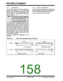
PIC16F/LF1946/47
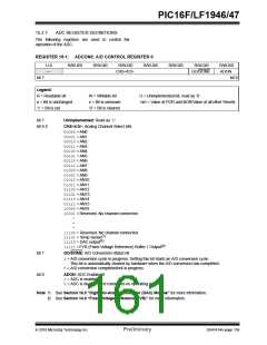
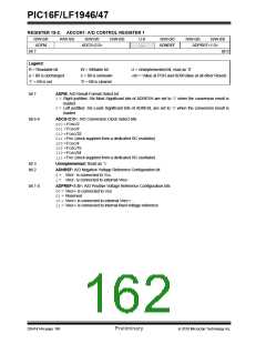
REGISTER 15-2: ADCON1: A/D CONTROL REGISTER 1
R/W-0/0
ADFM
R/W-0/0
R/W-0/0
R/W-0/0
U-0
—
R/W-0/0
R/W-0/0
R/W-0/0
ADCS<2:0>
ADNREF
ADPREF<1:0>
bit 7
bit 0
Legend:
R = Readable bit
W = Writable bit
U = Unimplemented bit, read as ‘0’
-n/n = Value at POR and BOR/Value at all other Resets
u = Bit is unchanged
‘1’ = Bit is set
x = Bit is unknown
‘0’ = Bit is cleared
bit 7
ADFM: A/D Result Format Select bit
1= Right justified. Six Most Significant bits of ADRESH are set to ‘0’ when the conversion result is
loaded.
0= Left justified. Six Least Significant bits of ADRESL are set to ‘0’ when the conversion result is
loaded.
bit 6-4
ADCS<2:0>: A/D Conversion Clock Select bits
000=FOSC/2
001=FOSC/8
010=FOSC/32
011=FRC (clock supplied from a dedicated RC oscillator)
100=FOSC/4
101=FOSC/16
110=FOSC/64
111=FRC (clock supplied from a dedicated RC oscillator)
bit 3
bit 2
Unimplemented: Read as ‘0’
ADNREF: A/D Negative Voltage Reference Configuration bit
0= VREF- is connected to VSS
1= VREF- is connected to external VREF-
bit 1-0
ADPREF<1:0>: A/D Positive Voltage Reference Configuration bits
00= VREF+ is connected to VDD
01= Reserved
10= VREF+ is connected to external VREF+
11= VREF+ is connected to internal fixed voltage reference
DS41414A-page 160
Preliminary
2010 Microchip Technology Inc.

 MICROCHIP [ MICROCHIP ]