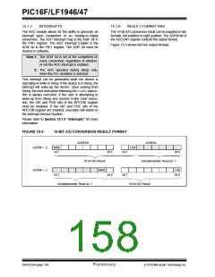
PIC16F/LF1946/47
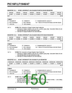
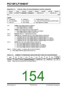
REGISTER 14-1: FVRCON: FIXED VOLTAGE REFERENCE CONTROL REGISTER
R/W-0/0
FVREN
R-q/q
FVRRDY(1)
R/W-0/0
R/W-0/0
R/W-0/0
R/W-0/0
R/W-0/0
R/W-0/0
Reserved
Reserved
CDAFVR<1:0>
ADFVR<1:0>
bit 7
bit 0
Legend:
R = Readable bit
W = Writable bit
U = Unimplemented bit, read as ‘0’
u = Bit is unchanged
‘1’ = Bit is set
x = Bit is unknown
‘0’ = Bit is cleared
-n/n = Value at POR and BOR/Value at all other Resets
q = Value depends on condition
bit 7
bit 6
FVREN: Fixed Voltage Reference Enable bit
0= Fixed Voltage Reference is disabled
1= Fixed Voltage Reference is enabled
FVRRDY: Fixed Voltage Reference Ready Flag bit(1)
0= Fixed Voltage Reference output is not ready or not enabled
1= Fixed Voltage Reference output is ready for use
bit 5-4
bit 3-2
Reserved: Read as ‘0’. Maintain these bits clear.
CDAFVR<1:0>: Comparator and DAC Fixed Voltage Reference Selection bit
00= Comparator and DAC Fixed Voltage Reference Peripheral output is off
01= Comparator and DAC Fixed Voltage Reference Peripheral output is 1x (1.024V)
10= Comparator and DAC Fixed Voltage Reference Peripheral output is 2x (2.048V)(2)
11= Comparator and DAC Fixed Voltage Reference Peripheral output is 4x (4.096V)(2)
bit 1-0
ADFVR<1:0>: ADC Fixed Voltage Reference Selection bit
00= ADC Fixed Voltage Reference Peripheral output is off
01= ADC Fixed Voltage Reference Peripheral output is 1x (1.024V)
10= ADC Fixed Voltage Reference Peripheral output is 2x (2.048V)(2)
11= ADC Fixed Voltage Reference Peripheral output is 4x (4.096V)(2)
Note 1: FVRRDY is always ‘1’ on devices with LDO (PIC16F1946/47).
2: Fixed Voltage Reference output cannot exceed VDD.
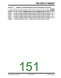
TABLE 14-1: SUMMARY OF REGISTERS ASSOCIATED WITH FIXED VOLTAGE REFERENCE
Register
on page
Name
Bit 7
Bit 6
Bit 5
Bit 4
Bit 3
Bit 2
Bit 1
Bit 0
FVRCON
FVREN
FVRRDY
Reserved Reserved
CDAFVR<1:0>
ADFVR<1:0>
152
Legend:
Shaded cells are not used with the Fixed Voltage Reference.
DS41414A-page 152
Preliminary
2010 Microchip Technology Inc.

 MICROCHIP [ MICROCHIP ]