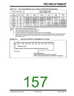
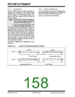
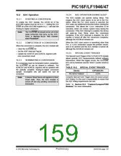
PIC16F/LF1946/47
15.2.7
ADC REGISTER DEFINITIONS
The following registers are used to control the
operation of the ADC.
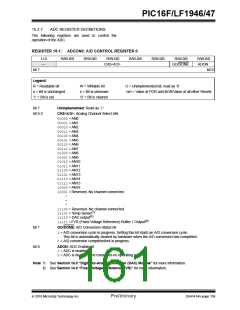
REGISTER 15-1: ADCON0: A/D CONTROL REGISTER 0
U-0
—
R/W-0/0
R/W-0/0
R/W-0/0
R/W-0/0
R/W-0/0
R/W-0/0
R/W-0/0
ADON
CHS<4:0>
GO/DONE
bit 7
bit 0
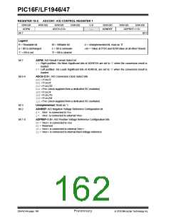
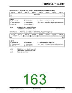
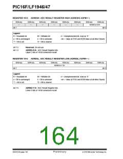
Legend:
R = Readable bit
W = Writable bit
U = Unimplemented bit, read as ‘0’
-n/n = Value at POR and BOR/Value at all other Resets
u = Bit is unchanged
‘1’ = Bit is set
x = Bit is unknown
‘0’ = Bit is cleared
bit 7
Unimplemented: Read as ‘0’
bit 6-2
CHS<4:0>: Analog Channel Select bits
00000= AN0
00001= AN1
00010= AN2
00011= AN3
00100= AN4
00101= AN5
00110= AN6
00111= AN7
01000= AN8
01001= AN9
01010= AN10
01011= AN11
01100= AN12
01101= AN13
01110= AN14
01111= AN15
10000= AN16
10001= Reserved. No channel connected.
•
•
•
11100= Reserved. No channel connected.
11101= Temp Sense(2)
11110= DAC output(1)
11111=FVR (Fixed Voltage Reference) Buffer 1 Output(2)
GO/DONE: A/D Conversion Status bit
bit 1
bit 0
1= A/D conversion cycle in progress. Setting this bit starts an A/D conversion cycle.
This bit is automatically cleared by hardware when the A/D conversion has completed.
0= A/D conversion completed/not in progress
ADON: ADC Enable bit
1= ADC is enabled
0= ADC is disabled and consumes no operating current
Note 1: See Section 16.0 “Digital-to-Analog Converter (DAC) Module” for more information.
2: See Section 14.0 “Fixed Voltage Reference (FVR)” for more information.
2010 Microchip Technology Inc.
Preliminary
DS41414A-page 159

 MICROCHIP [ MICROCHIP ]