PIC16F/LF1946/47
14.1 Independent Gain Amplifiers
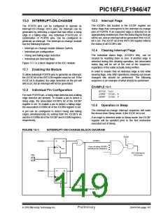
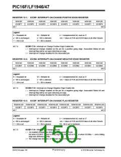
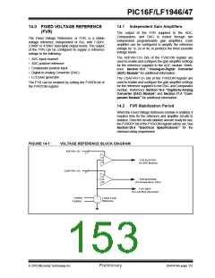
14.0 FIXED VOLTAGE REFERENCE
(FVR)
The output of the FVR supplied to the ADC,
Comparators, and DAC is routed through two
independent programmable gain amplifiers. Each
amplifier can be configured to amplify the reference
voltage by 1x, 2x or 4x, to produce the three possible
voltage levels.
The Fixed Voltage Reference, or FVR, is a stable
voltage reference, independent of VDD, with 1.024V,
2.048V or 4.096V selectable output levels. The output
of the FVR can be configured to supply a reference
voltage to the following:
The ADFVR<1:0> bits of the FVRCON register are
used to enable and configure the gain amplifier settings
for the reference supplied to the ADC module. Refer-
ence Section 15.0 “Analog-to-Digital Converter
(ADC) Module” for additional information.
• ADC input channel
• ADC positive reference
• Comparator positive input
• Digital-to-Analog Converter (DAC)
• LCD bias generator
The CDAFVR<1:0> bits of the FVRCON register are
used to enable and configure the gain amplifier settings
for the reference supplied to the DAC and Comparator
module. Reference Section 16.0 “Digital-to-Analog
Converter (DAC) Module” and Section 17.0 “Com-
parator Module” for additional information.
The FVR can be enabled by setting the FVREN bit of
the FVRCON register.
14.2 FVR Stabilization Period
When the Fixed Voltage Reference module is enabled, it
requires time for the reference and amplifier circuits to
stabilize. Once the circuits stabilize and are ready for use,
the FVRRDY bit of the FVRCON register will be set. See
Section 29.0 “Electrical Specifications” for the
minimum delay requirement.
FIGURE 14-1:
VOLTAGE REFERENCE BLOCK DIAGRAM
ADFVR<1:0>
2
X1
X2
X4
FVR BUFFER1
(To ADC Module)
CDAFVR<1:0>
2
X1
X2
X4
FVR BUFFER2
(To Comparators, DAC)
FVR VREF
(To LCD Bias Generator)
+
_
FVREN
FVRRDY
1.024V Fixed
Reference
2010 Microchip Technology Inc.
Preliminary
DS41414A-page 151

 MICROCHIP [ MICROCHIP ]