3 .0 V/3 .3 V Ad ju s t a b le Mic ro p ro c e s s o r
S u p e rvis o ry Circ u it s
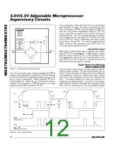
The propagation delay through the CE transmission
gate depends on V , the source impedance of the
CC
drive connected to CE IN, and the loading on CE OUT
(see the Chip-Enable Propagation Delay vs. CE OUT
Loa d Ca p a c ita nc e g ra p h in the Typ ic a l Op e ra ting
Characteristics). The CE propagation delay is produc-
tion tested from the 50% point on CE IN to the 50%
point on CE OUT using a 50Ω driver and 50pF of load
c a pa c ita nc e (Figure 9). For minimum p ropa ga tion
delay, minimize the capacitive load at CE OUT, and
use a low-output-impedance driver.
MAX793
MAX794
MAX795
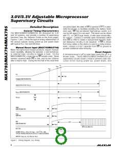
OUT
P
CHIP-ENABLE
OUTPUT
CONTROL
RESET
GENERATOR
P
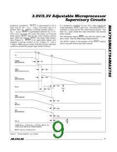
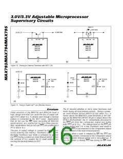
Chip-Enable Output
When the CE transmission gate is enabled, the imped-
ance of CE OUT is equivalent to a 46Ω resistor in series
with the source driving CE IN. In the disabled mode,
the transmission gate is off and an active pull-up con-
nects CE OUT to OUT (Figure 8). This pull-up turns off
when the transmission gate is enabled.
CE IN
CE OUT
N
Ea rly P o w e r-Fa il Wa rn in g
(MAX7 9 3 /MAX7 9 4 )
Figure 7. Chip-Enable Transmission Gate
Critical systems often require an early warning indicat-
ing that power is failing. This warning provides time for
the µP to store vital data and take care of any additional
“housekeeping” functions, before the power supply
gets too far out of tolerance for the µP to operate reli-
a b ly. The MAX793/MAX794 offe r two me thod s of
achieving this early warning. If access to the unregu-
lated supply is feasible, the power-fail comparator input
(PFI) c a n b e c onne c te d to the unre g ula te d s up p ly
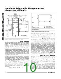
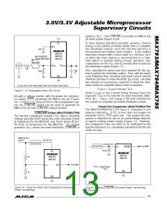
The CE transmission gate remains disabled and CE IN
remains high impedance (regardless of CE IN activity)
for the first half of the reset timeout period (t / 2), any
time a reset is generated. While disabled, CE IN is
high impedance. When the CE transmission gate is
enabled, the impedance of CE IN appears as a 46Ω
resistor in series with the load at CE OUT.
34/MAX795
RP
V
RST
V
RST
V
RST
V
RST
V
CC
V
SW
V
SW
CE OUT
V
BATT
V
BATT
10µs
V
CC
t
RP
/2
t
RP
RESET
(PULLED TO V
)
CC
CE IN
V
BATT
= 3.6V
RESET PULLED UP TO V
CC
Figure 8. Chip-Enable Timing
12 ______________________________________________________________________________________

 MAXIM [ MAXIM INTEGRATED PRODUCTS ]