3 .0 V/3 .3 V Ad ju s t a b le Mic ro p ro c e s s o r
S u p e rvis o ry Circ u it s
34/MAX795
V
RST
V
CC
V
CC
4.7k
MAX793/MAX794
t
RP
WDO
TO µP
RESET
RESET
WDO
MR
V
CC
t
WD
WDI
10µs
WDO
RESET
WDI
t
RP
t
WP
t
RP
WDO CONNECTED TO µP INTERRUPT
RESET PULLED UP TO V
CC
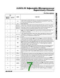
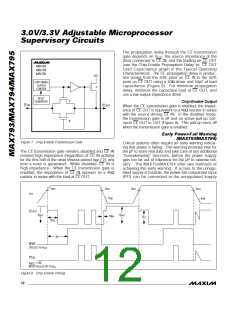
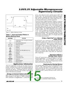
Figure 5. Watchdog Timing Relationship
either when a reset occurs or when a transition (low-to-
high or high-to-low) takes place at WDI. As long as
reset is asserted, the timer remains cleared and does
not c ount. As s oon a s re s e t is re le a s e d or WDI
changes state, the timer starts counting (Figure 5).
WDI can detect pulses as short as 100ns. Unlike the
5V MAX690 family, the watchdog function cannot be
disabled.
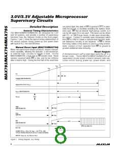
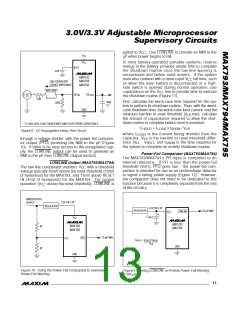
Figure 6. Generating a Reset on Each Watchdog Fault
Ch ip -En a b le S ig n a l Ga t in g
Internal gating of chip-enable (CE) signals prevents erro-
neous data from corrupting CMOS RAM in the event of an
undervoltage condition. The MAX793/MAX794/MAX795
use a series transmission gate from CE IN to CE OUT
(Figure 7). During normal operation (reset not asserted),
the CE transmission gate is enabled and passes all CE
transitions. When reset is asserted, this path becomes
disabled, preventing erroneous data from corrupting the
CMOS RAM. The short CE propagation delay from CE IN
to CE OUT enables these µP supervisors to be used with
most µPs. If CE IN is low when reset asserts, CE OUT
remains low for typically 10µs to permit completion of the
current write cycle.
Wa t c h d o g Ou t p u t (MAX7 9 3 /MAX7 9 4 )
In the MAX793/MAX794, WDO remains high (WDO is
pulled up to V ) if there is a transition or pulse at WDI
CC
during the watchdog timeout period. WDO goes low if
no transition occurs at WDI during the watchdog timeout
period. The watchdog function is disabled and WDO is
a logic high when reset is asserted if V is above V
.
CC
SW
WDO is a logic low when V is below V
.
CC
SW
Chip-Enable Input
The CE transmission gate is disabled and CE IN is high
impedance (disabled mode) while reset is asserted.
If a system reset is desired on every watchdog fault,
s imp ly d iod e -OR c onne c t WDO to MR (Fig ure 6).
When a watchdog fault occurs in this mode, WDO goes
low, pulling MR low, which causes a reset pulse to be
issued. Ten microseconds after reset is asserted, the
watchdog timer clears and WDO returns high. This
delay results in a 10µs pulse at WDO, allowing external
During a power-down sequence when V
passes the
CC
reset threshold, the CE transmission gate disables and
CE IN immediately becomes high impedance if the volt-
a g e a t CE IN is hig h. If CE IN is low whe n re s e t
asserts, the CE transmission gate will disable at the
moment CE IN goes high, or 10µs after reset asserts,
whichever occurs first (Figure 8). This permits the cur-
rent write cycle to complete during power-down.
circuitry to “capture” a watchdog fault indication.
A
continuous high or low on WDI will cause 200ms reset
pulses to be issued every 1.6sec.
______________________________________________________________________________________ 11

 MAXIM [ MAXIM INTEGRATED PRODUCTS ]