3 .0 V/3 .3 V Ad ju s t a b le Mic ro p ro c e s s o r
S u p e rvis o ry Circ u it s
34/MAX795
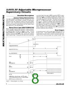
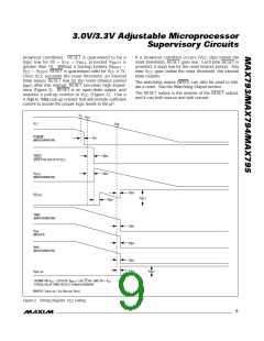
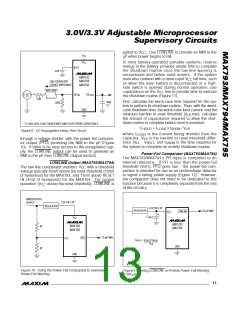
brownout conditions. RESET is guaranteed to be a
If a brownout condition occurs (V
dips below the
CC
log ic low for 0V < V
greater than 1V. Without a backup battery (V
< V
, p rovid e d V
is
=
reset threshold), RESET goes low. Each time RESET is
asserted, it stays low for the reset timeout period. Any
CC
RST
BATT
BATT
V
CC
= V
), RESET is guaranteed valid for V ≥ 1V.
time V
goes below the reset threshold, the internal
OUT
CC
CC
Once V
exceeds the reset threshold, an internal
timer restarts.
CC
timer keeps RESET low for the reset timeout period
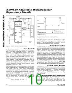
The watchdog output (WDO) can also be used to initi-
ate a reset. See the Watchdog Output section.
(t ); after this interval, RESET becomes high imped-
RP
ance (Figure 2). RESET is an open-drain output, and
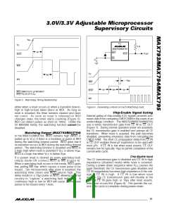
The RESET output is the inverse of the RESET output,
and it can both source and sink current.
requires a pull-up resistor to V
(Figure 3). Use a
CC
4.7kΩ to 1MΩ pull-up resistor that will provide sufficient
current to assure the proper logic levels to the µP.
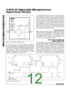
V
LL
V
RST
V
CC
V
SW
V
LOWLINE
4µs
(MAX793/MAX794)
V
RESET
20µs
20µs
(RESET PULLED UP TO V
)
CC
V
RESET
(MAX793/MAX794)
25µs
V
CE OUT
V
BATT
10µs
V
WDO
(MAX793/MAX794)
25µs
25µs
V
BOK
(MAX793)
V
PFO
(MAX793/MAX794)
25µs
25µs
V
BATT
V
BATT ON
SHOWN FOR V = 3.3V to 0V, V
= 3.6V, CE IN = GND, PFI = V .
CC
CC
BATT
TYPICAL DELAY TIMES REFLECT A 40mV OVERDRIVE
MAX794: V = V (V / V
)
RESET IN CC RST IN RST
Figure 2. Timing Diagram, V Falling
CC
_______________________________________________________________________________________
9

 MAXIM [ MAXIM INTEGRATED PRODUCTS ]