3 .0 V/3 .3 V Ad ju s t a b le Mic ro p ro c e s s o r
S u p e rvis o ry Circ u it s
V
IN
3.0V OR 3.3V
3.0V OR 3.3V
V
V
CC
CC
R1
R2
R1
R2
MAX793
MAX794
MAX793
MAX794
PFI
PFO
PFI
PFO
MR
GND
GND
V
IN
V
CC
V
CC
PFO
PFO
V
IN
V
IN
V
L
V
TRIP
V
TRIP
V
H
0V
1
1
V
CC
R1 + R2
R2
+
–
V
= R2 (V + V
PFT
)
TRIP
PFH
V
= V
PFT
(
)
CC
TRIP
(
)
R1 R2
R1
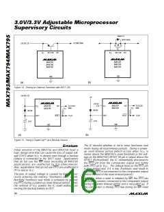
WHERE V = 1.237V
PFT
1
1
V
V
PFH
= 10mV
R1 + R2
+
–
V = R2 (V
)
L
PFT
V = (V + V
)
(
)
H
PFT PFH
(
)
R1 R2
R1
NOTE: V
TRIP,
V ARE NEGATIVE
L
R2
(a)
(b)
Figure 12. Using the Power-Fail Comparator to Monitor an Additional Power Supply: (a) V Is Negative, (b) V Is Positive
IN
IN
34/MAX795
The power-fail comparator turns off and PFO goes low
when V falls below V on power-down. During the
V
is greater than V , or when V
falls below
BATT
CC
CC
1.75V (typ) regardless of the BATT voltage.
CC
SW
first half of the reset timeout period (t ), PFO is forced
RP
Switchover at V ensures that battery-backup mode is
SW
high, irrespective of V . At the beginning of the sec-
PFI
entered before V
gets too close to the 2.0V mini-
OUT
ond half of t , the power-fail comparator is enabled
RP
mum required to reliably retain data in most CMOS
RAM, (s witc hove r a t hig he r V volta g e s would
and PFO follows PFI. If the comparator is unused, con-
nect PFI to VCC and leave PFO unconnected. PFO may
be connected to MR so that a low voltage on PFI will
generate a reset (Figure 12b). In this configuration,
when the monitored voltage causes PFI to fall below
CC
decrease backup-battery life). When V
recovers,
CC
switchover is deferred either until V crosses V
if
CC
BATT
V
BATT
is below V
, or when V
rises above the
RST
CC
reset threshold (V
powe r-up switc hove r te c hnique p re ve nts V
) if V
is above V .
This
from
RST
BATT
RST
V , PFO pulls MR low, causing a reset to be assert-
PFT
CC
ed. Reset remains asserted as long as PFO holds MR
low, and for 200ms after PFO pulls MR high when the
monitored supply is above the programmed threshold.
charging the backup battery through OUT when using
an external transistor driven by BATT ON. OUT con-
nects to V
through a 4Ω (max) PMOS power switch
CC
when V crosses the reset threshold (Figure 13).
CC
Ba c k u p -Ba t t e ry S w it c h o ve r
In the event of a brownout or power failure, it may be
necessary to preserve the contents of RAM. With a
backup battery installed at BATT, the devices automati-
BATT ON (MAX7 9 3 /MAX7 9 4 )
BATT ON is high when OUT is connected to BATT.
Although BATT ON can be used as a logic output to
indicate the battery switchover status, it is most often
used as a gate or base drive for an external pass tran-
sistor for high-c urre nt a pp lic a tions (se e Driving a n
Exte rna l Switc h with BATT ON in the Ap p lic a tions
cally switch RAM to backup power when V
falls. In
CC
order to allow the backup battery (e.g., a 3.6V lithium
cell) to have a higher voltage than V , this family of µP
CC
supervisors (designed for 3.3V and 3V systems) does
not a lwa ys c onne c t BATT to OUT whe n V
is
BATT
Informa tion s e c tion). Whe n V
e xc e e d s V
on
CC
RST
greater than V
.
BATT connects to OUT (through a
CC
power-up, BATT ON sinks 3.2mA at 0.4V. In battery-
backup mode, this terminal sources 100µA from BATT.
140Ω switch) either when V falls below V and
CC
SW
14 ______________________________________________________________________________________

 MAXIM [ MAXIM INTEGRATED PRODUCTS ]