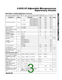
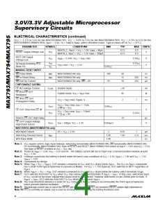
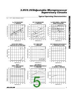
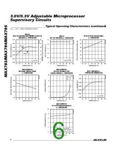
3 .0 V/3 .3 V Ad ju s t a b le Mic ro p ro c e s s o r
S u p e rvis o ry Circ u it s
34/MAX795
______________________________________________________________P in De s c rip t io n
PIN
NAME
FUNCTION
MAX793/
MAX794
MAX795
Supply Output for CMOS RAM. When V rises above the reset threshold or above
CC
1
2
1
2
OUT
V
V
CC
, OUT is connected to V through an internal P-channel MOSFET switch. When
BATT CC
falls below V and V
, BATT connects to OUT.
SW
BATT
V
CC
Main Supply Input
BATT OK
(MAX793)
Battery Status Output. High in normal operating mode when V
exceeds V
, other-
BATT
BOK
wise low. V
is checked continuously. Disabled and logic low while V is below V
.
BATT
CC
SW
3
4
—
—
RESET IN
(MAX794)
Reset Input. Connect to an external resistor divider to select the reset threshold. The
reset threshold can be programmed anywhere in the V to 5.5V range.
SW
Power-Fail Comparator Input. When PFI is less than V
or when V falls below V
,
PFT
CC
SW
PFI
PFO goes low; otherwise, PFO remains high (see Power-Fail Comparator section).
Connect to V if unused.
CC
Logic Output/External Bypass Switch-Driver Output. High when OUT switches to BATT.
Low when OUT switches to V . Connect the base/gate of PNP/PMOS transistor to
5
6
7
3
4
BATT ON
GND
CC
BATT ON for I
requirements exceeding 75mA.
OUT
Ground
Power-Fail Comparator Output. When PFI is less than V
or when V falls below
CC
PFT
—
PFO
V , PFO goes low; otherwise, PFO remains high. PFO is also used to enable the bat-
SW
tery freshness seal (see Battery Freshness Seal, and Power-Fail Comparator sections).
Manual Reset Input. A logic low on MR asserts reset. Reset remains asserted as long as
MR is low and for 200ms after MR returns high. The active-low input has an internal
70µA pull-up current. In can be driven from a TTL- or CMOS-logic line or shorted to
ground with a switch. Leave open if unused.
8
9
—
—
—
MR
WDO
WDI
Watchdog Output. WDO goes low if WDI remains either high or low for longer than the
watchdog timeout period. WDO returns high on the next transition of WDI. WDO is a
logic high for V < V < V , and low when V is below V .
SW
SW
CC
RST
CC
Watchdog Input. If WDI remains either high or low for longer than the watchdog timeout
period, the internal watchdog timer runs out and WDO goes low. WDO returns high on
the next transition of WDI. Connect WDO to MR to generate a reset due to a watchdog
fault.
10
11
12
5
6
CE IN
Chip-Enable Input. The input to the chip-enable gating circuit. Connect to GND if unused
Chip-Enable Output. CE OUT goes low only when CE IN is low and reset is not asserted.
If CE IN is low when reset is asserted, CE OUT will remain low for 10µs or until CE IN
goes high, whichever occurs first. CE OUT is pulled up to OUT.
CE OUT
13
14
—
—
RESET
Active-High Reset Output. Sources and sinks current. RESET is the inverse of RESET.
Early Power-Fail Warning Output. Low when V falls to V . This output can be used to
CC
LR
LOWLINE
generate an NMI to provide early warning of imminent power-failure.
Open-Drain, Active-Low Reset Output. Pulses low for 200ms when triggered, and stays
low whenever V is below the reset threshold or when MR is a logic low. It remains low
for 200ms after either V rises above the reset threshold, the watchdog triggers a reset
CC
(WDO connected to MR), or MR goes low to high.
CC
15
16
7
8
RESET
BATT
Backup-Battery Input. When V falls below V and V
, OUT switches from V to
BATT CC
CC
SW
BATT. When V rises above the reset threshold or above V
, OUT reconnects to
BATT
CC
V
. V
may exceed V . Connect V , OUT, and BATT together if no battery is
CC CC
CC BATT
used.
_______________________________________________________________________________________
7

 MAXIM [ MAXIM INTEGRATED PRODUCTS ]