Trip le -Ou t p u t P o w e r-S u p p ly
Co n t ro lle r fo r No t e b o o k Co m p u t e rs
MAX782
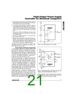
5. Keep the gate connections to the MOSFETs short for
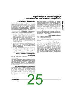
+5V
SUPPLY
low inductance (less than 20mm long and more than
0.5mm wide) to ensure clean switching.
6. To achieve good shielding, it is best to keep all
high-voltage switching signals (MOSFET gate dri-
ves DH3 and DH5, BST3 and BST5, and the two LX
nodes) on one side of the board and all sensitive
nodes (CS3, CS5, FB3, FB5 and REF) on the other
side.
FB5
D_
1M
R1
R2
MAX782
Q_
+5V
POWER-READY
7. Connect the GND and PGND pins directly to the
ground plane, which should ideally be an inner layer
of a multilayer board.
1.65V
604k
8. Connect the bypass capacitor C2 very close (less
than 10mm) to the VL pin.
9. Minimize the capacitance at the transformer sec-
ondary. Place D5 and C12 very close to each other
and to the secondary, then route the output to the IC’s
VDD pin with a short trace. Bypass with 0.1µF close
to the VDD pin if this trace is longer than 50mm.
GND
The layout for the evaluation board is shown in the
Evaluation Kit section. It provides an effective, low-
noise, high-efficiency example.
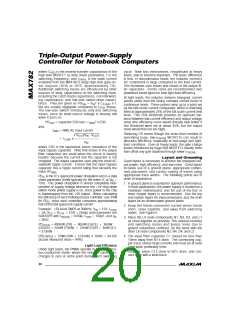
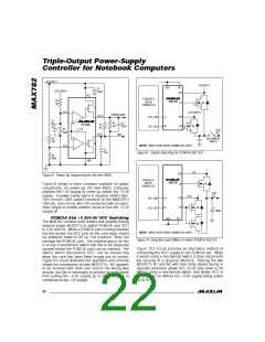
Figure 6. Power-Ready Signal for the +5V Supply
P o w e r-Re a d y a n d P o w e r S e q u e n c in g
A “power-ready” signal can be generated from one of
the comparator outputs by connecting one of the sup-
plies (e.g., the +5V output – see Figure 6) through a
high-resistance voltage divider to the comparator input.
The threshold for the +5V-output comparator is set by
+5V
SUPPLY
V
CC
+3.3V
SUPPLY
RESET
R1 and R2 according to the formula: V = 1.65V x (R1
POWER READY
POWER READY
TH
+ R2) / R2. For example, choosing R1 = 1MΩ and R2 =
604kΩ sets the nominal threshold to 4.38V.
R1
1.24M
RESET
MR
RESET
4.65V
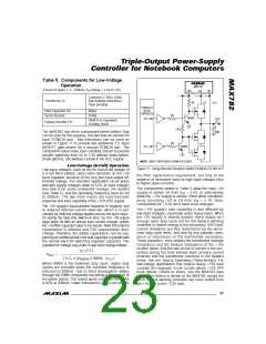
If the power-ready signal is required to indicate when
both the +3.3V and the +5V supplies have come up,
use the MAX707 supervisory circuit shown in Figure 7.
The threshold for the +3.3V-line comparator is set by
PFI
R1 and R2 according to the formula: V = 1.25V x (R1
PFO
TH
R2
1M
+ R2) / R2. For example, choosing R1 = 1.2MΩ and R2
= 1MΩ sets the nominal threshold to 2.75V. The thresh-
old for the +5V supply is preset inside the MAX707,
and is typically 4.65V. The reset outputs remain assert-
ed while either supply line is below its threshold, and
for at least 140ms after both lines are fully up.
1.25V
GND
MAX707
If sequencing of the +3.3V and +5V supplies is critical,
several approaches are possible. For example, the
SS3 and SS5 capacitors can be sized to ensure that
the two supplies come up in the desired order. This
technique requires that the SS capacitors be selected
specifically for each individual situation, because the
loading on each supply affects its power-up speed.
Figure 7. Power-Ready Signal Covers Both +3.3V and +5V
Supplies with External Voltage Monitor IC (MAX707)
Another approach uses the “power-ready” comparator
output signal (see Figure 6) from one supply as a con-
trol input to the ON_ pin of the other supply.
______________________________________________________________________________________ 21

 MAXIM [ MAXIM INTEGRATED PRODUCTS ]