Trip le -Ou t p u t P o w e r-S u p p ly
Co n t ro lle r fo r No t e b o o k Co m p u t e rs
MAX782
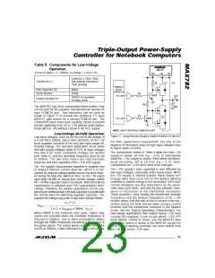
Table 5. Components for Low-Voltage
Operation
MAX782
FB5
(Circuit of Figure 1, f = 200kHz, VIN Range = 5.5V to 12V)
VDD
FB3
Coiltronics CTX03-12062
Transformer L2:
(low-leakage inductance,
10µH primary)
1M
+5V
+3.3V
PCMCIA 2.0
DIGITAL
CONTROLLER
Filter Capacitor C6:
Sense Resistor:
660µF
1M
25mΩ
2N3904
VCC_EN0
SLOT
VCC
1N5819 or equivalent
Schottky diode
Flyback Rectifier D2:
510k
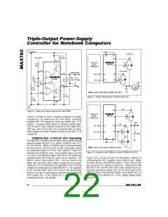
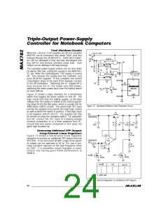
The MAX782 has three comparators/level-shifters that
can be used for this purpose, and two that are needed for
each PCMCIA port. Two transistors can be used as
shown in Figure 11 to provide two additional TTL-input
MOSFET gate drivers for a second PCMCIA slot. The
component values have been carefully chosen to provide
smooth switching from 5V to 3.3V without make-before-
break glitches, and without a break in the VCC supply.
100µF
1M
2N3904
VCC_EN1
NOTE: MOSFET BODY DIODES SHOWN FOR CLARITY.
Lo w -Vo lt a g e (6 -Ce ll) Op e ra t io n
Low input voltages, such as the 6V end-of-life voltage of
a 6-cell NiCd battery, place extra demands on the +5V
buck regulator because of the very low input-output dif-
ferential voltage. The standard application circuit works
well with supply voltages down to 6.5V; at input voltages
less than 6.5V, some component changes are needed
(see Table 5), and the operating frequency must be set
to 200kHz. The two ma in is s ue s a re loa d -tra ns ie nt
response and load capability of the +15V VDD supply.
Figure 11. Using Discrete Circuitry to Switch PCMCIA 2.0 Slot VCC
the filte r c a p a c ita nc e re q uire me nt, b ut only a t the
expense of increased noise at high input voltages (due
to higher peak currents).
The components shown in Table 5 allow the main +5V
supply to deliver 2A from V = 5.5V, or alternatively
IN
allow the +15V supply to deliver 70mA while simultane-
ous ly p rovid ing + 5V a t 2A from V = 5.7V. Note :
IN
Components for +3.3V don’t need to be changed.
The +5V supply’s load-transient response is impaired due
to reduced inductor-current slew rate, which is in turn
caused by reduced voltage applied across the buck induc-
tor during the high-side switch-on time. So, the +5V output
sags when hit with an abrupt load current change, unless
the +5V filter capacitor value is increased. Note that only the
capacitance is affected and ESR requirements don’t
change. Therefore, the added capacitance can be sup-
plied by an additional low-cost bulk capacitor in parallel with
the normal low-ESR switching-regulator capacitor. The
equation for voltage sag under a step-load change follows:
The +15V supply’s load capability is also affected by
low input voltages, especially under heavy loads. When
the +5V supply is heavily loaded, there simply isn’t
enough extra duty cycle left for the flyback winding
controller to deliver energy to the secondary. VDD load-
current limitations are thus determined by the worst-
case duty-cycle limits, and also by any parasitic resis-
tance or inductance on the transformer secondary.
These parasitics, most notably the transformer leakage
inductance and the forward impedance of the +15V
rectifier diode, limit the rate-of-rise of current in the sec-
ondary during the brief interval when primary current
reverses and the transformer conducts in the forward
mode. See the Typical Operating Characteristics. For
low-voltage applications that require heavy +15V load
currents (for example, 6-cell circuits where +12V VPP
must deliver 120mA or more), see the MAX783 data
sheet. This device is similar to the MAX782 except the
+15V flyback winding controller has been shifted from
the +5V side to the +3.3V side.
2
I
x L
STEP
V
SAG
= —————————————————
2 x C x (V
x DMAX - V
)
F
IN(MIN)
OUT
where DMAX is the maximum duty cycle. Higher duty
cycles are possible when the oscillator frequency is
reduced to 200kHz, due to fixed propagation delays
through the PWM comparator becoming a lesser part of
the whole period. The tested worst-case limit for DMAX
is 92% at 200kHz. Lower inductance values can reduce
______________________________________________________________________________________ 23

 MAXIM [ MAXIM INTEGRATED PRODUCTS ]