Trip le -Ou t p u t P o w e r-S u p p ly
Co n t ro lle r fo r No t e b o o k Co m p u t e rs
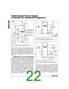
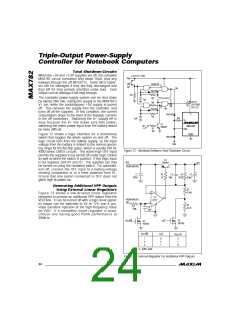
To t a l S h u t d o w n Circ u it s
When the +5V and +3.3V supplies are off, the complete
(+5.5V TO +18V)
BATT
V
MAX782 circuit consumes only about 70µA, plus any
leakage through the off MOSFETs. Some NiCd batter-
ies can be damaged if they are fully discharged and
then left for long periods (months) under load. Even
100µA can do damage if left long enough.
CD4011B
1N4148
ON/
OFF
S
ON
1M
The complete power-supply system can be shut down
by taking ON5 low, cutting the supply to the MAX782’s
V+ pin, while the bootstrapped +5V supply is turned
off. This removes the supply from the controller, and
turns off all the supplies. In this condition, the current
consumption drops to the level of the leakage currents
in the off transistors. Switching the V+ supply off is
e a s y b e c a us e the V+ line d ra ws ve ry little p owe r;
switching the entire power input from the battery would
be more difficult.
MAX782
1M
1M
1µF
ZETEX
ZVP2106G
SOT 223
ON
R
1N4148
1M
V+
1N4148
1M
1µF
VL
Q1
2N4401
OFF
MAX782
R1
1M
ON5
Figure 12 shows a logic interface for a momentary
switch that toggles the whole system on and off. The
logic circuit runs from the battery supply, so the input
voltage from the battery is limited to the normal operat-
ing range for the flip-flop gates, which is usually 18V for
4000-series CMOS circuits. The active-high OFF input
permits the supplies to be turned off under logic control
as well as when the switch is pushed. If this logic input
is not required, omit R1 and Q1. The supplies can only
be turned on using the hardware switch. For automatic
turn-off, connect the OFF input to a battery-voltage
sensing comparator or to a timer powered from VL.
Ensure that any signal connected to OFF does not
glitch high at power-up.
PGND
1N4148
ON5
Figure 12. Hardware/Software Total Shutdown Circuit
Q1
2N4403
VDD
OUT
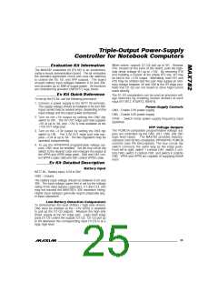
FROM MAX782
C1
100nF
R4
1k
C3
10nF
R1
16.9k
C2
6.8µF
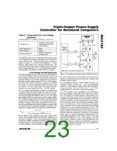
Ge n e ra t in g Ad d it io n a l VP P Ou t p u t s
Us in g Ex t e rn a l Lin e a r Re g u la t o rs
R2
6.34k
3
2
7
Fig ure 13 s hows a low-d rop out line a r re g ula tor
designed to provide an additional VPP output from the
VDD line. It can be turned off with a logic-level signal;
its output can be switched to 5V or 12V; and it pro-
vides excellent rejection of the high-frequency noise
on VDD. If a monolithic line a r re g ula tor is us e d ,
c hoos e one ha ving g ood PSRR p e rforma nc e a t
300kHz.
U1
OP27
6
FROM MAX782
REF
4
R3
26.7k
R5
100k
C4
10nF
Q3
2N7002
OFF/ON
12/5
Q2
2N7002
OFF/ON
12/5
V
OUT
(V)
1
0
0
X
0
1
0
5
12
X = DON'T CARE
Figure 13. External Regulator For Additional VPP Outputs
24 ______________________________________________________________________________________

 MAXIM [ MAXIM INTEGRATED PRODUCTS ]