Trip le -Ou t p u t P o w e r-S u p p ly
Co n t ro lle r fo r No t e b o o k Co m p u t e rs
where C
is the reverse transfer capacitance of the
cycle. New loss mechanisms, insignificant at heavy
loads, start to become important. The basic difference
is that, in discontinuous mode, the inductor current’s
AC component is large compared to the load current.
This increases core losses and losses in the output fil-
ter capacitors. Ferrite cores are recommended over
powdered toroid types for best light-load efficiency.
RSS
high-side MOSFET (a data sheet parameter), f is the
switching frequency, and I is the peak current
DRIVE
available from the MAX782’s large high-side gate dri-
ve r o u tp u ts (DH5 o r DH3 , a p p ro xim a te ly 1 A).
Additional switching losses are introduced by other
sources of stray capacitance at the switching node,
including the catch diode capacitance, coil interwind-
ing capacitance, and low-side switch-drain capaci-
tance. They are given as PD
but are usually negligible compared to C
At light loads, the inductor delivers triangular current
pulses rather than the nearly constant current found in
continuous mode. These pulses ramp up to a point set
by the idle-mode current comparator, which is internally
fixed at approximately 25% of the full-scale current-limit
level. This 25% threshold provides an optimum bal-
ance between low-current efficiency and output voltage
noise (the efficiency curve would actually look better if
this threshold were set at about 45%, but the output
noise would then be too high).
MAX782
2
= V
x C
x f,
SW
IN
STRAY
losses.
RSS
The low-s id e s witc h introd uc e s only tiny s witc hing
losses, since its drain-source voltage is already low
when it turns on.
2
PD
= capacitor ESR loss = I
x ESR
CAP
RMS
and,
I
= RMS AC input current
RMS
2
Reducing I R losses though the brute-force method of
√ V
(V - V
)
OUT IN
OUT
specifying huge, low-r
MOSFETs can result in
DS(ON)
= I
x ————————
LOAD
atrocious efficiency, especially at mid-range and light-
load conditions. Even at heavy loads, the gate charge
losses introduced by huge 50A MOSFETs usually more
V
IN
where ESR is the equivalent series resistance of the
input bypass capacitor. Note that losses in the output
filter capacitors are small when the circuit is heavily
loaded, because the current into the capacitor is not
chopped. The output capacitor sees only the small AC
sawtooth ripple current. Ensure that the input bypass
capacitor has a ripple current rating that exceeds the
than offset any gain obtained through lower r
.
DS(ON)
La yo u t a n d Gro u n d in g
Good layout is necessary to achieve the designed out-
put power, high efficiency, and low noise. Good layout
includes use of a ground plane, appropriate compo-
nent placement, and correct routing of traces using
appropriate trace widths. The following points are in
order of importance:
value of I
.
RMS
PD is the IC’s quiescent power dissipation and is a data
IC
sheet parameter (6mW typically for the entire IC at V
=
IN
15V). This power dissipation is almost completely inde-
pendent of supply voltage whenever the +5V step-down
switch-mode power supply is on, since power to the chip
is bootstrapped from the +5V output. When calculating
the efficiency of each individual buck controller, use 3mW
1. A ground plane is essential for optimum performance.
In most applications, the power supply is located on a
multilayer motherboard, and full use of the four or
more copper layers is recommended. Use the top
and bottom layers for interconnections, and the inner
layers for an uninterrupted ground plane.
for PD , since each controller consumes approximately
IC
half of the total quiescent supply current.
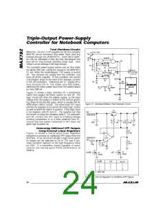
2. Keep the Kelvin-connected current-sense traces
s hort, c los e tog e the r, a nd a wa y from s witc hing
nodes. See Figure 5.
Example: +5V buck SMPS at 300kHz, V = 15V, I
IN
LOAD
= 2A, R = R
= ESR = 25mΩ, both transistors are
CS
COIL
Si9410DY with r
= 30nC.
= 0.05Ω, C
= 160pF, and q
RSS G
DS(ON)
3. Place the LX node components N1, N3, D3, and L1
as close together as possible. This reduces resistive
a nd s witc hing los s e s a nd ke e p s nois e d ue to
ground inductance confined. Do the same with the
other LX node components N2, N4, D4, and L2.
2
PD
= 400mW (I R) + 90mW (GATE) + 36mW
TOTAL
(DIODE) + 22mW (TRAN) + 22mW (CAP) + 3mW (IC)
= 573mW
Efficiency = 10W/(10W + 573mW) x 100% = 94.6%
(actual measured value = 94%).
4. The input filter capacitor C1 should be less than
10mm away from N1’s drain. The connecting cop-
per trace carries large currents and must be at least
2mm wide, preferably 5mm.
Light-Load Efficiency
Under light loads, the PWMs operate in the discontinu-
ous-conduction mode, where the inductor current dis-
charges to zero at some point during each switching
Similarly, place C13 close to N2’s drain, and con-
nect them with a wide trace.
20 ______________________________________________________________________________________

 MAXIM [ MAXIM INTEGRATED PRODUCTS ]