Trip le -Ou t p u t P o w e r-S u p p ly
Co n t ro lle r fo r No t e b o o k Co m p u t e rs
MAX782
The output ripple in continuous-current mode is:
V
= I x (ESR +1/(2 x π x f x C )).
LPP(MAX) CF F
OUT(RPL)
In idle-mode, the ripple has a capacitive and resistive
component:
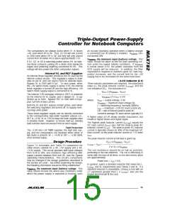
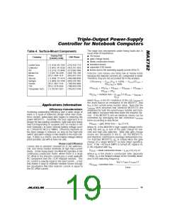
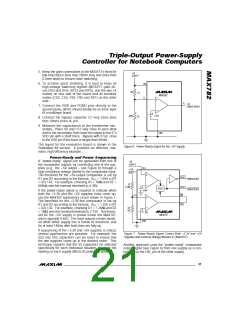
FAT, HIGH-CURRENT TRACES
MAIN CURRENT PATH
-4
4 x 10 x L
V
(C) = ——————— x
OUT(RPL)
2
R
CS
x C
F
SENSE RESISTOR
1
1
KELVIN SENSE TRACES
——— + ————— Volts
V
OUT
(
)
V - V
IN OUT
0.02 x ESR
CF
V
(R) = ——————- Volts
OUT(RPL)
R
CS
The total ripple, V
lows:
, can be approximated as fol-
OUT(RPL)
MAX782
if V
(R) < 0.5 V (C),
OUT(RPL)
OUT(RPL)
then V
= V
(C),
OUT(RPL)
OUT(RPL)
otherwise, V
V
= 0.5 V
(R).
(C) +
OUT(RPL)
OUT(RPL)
OUT(RPL)
Figure 5. Kelvin Connections for the Current-Sense Resistors
MOSFETs with low gate-threshold voltage specifica-
Dio d e D2
The voltage rating of D2 should be at least 2 x V
+
IN
tions (i.e., maximum V
= 2V rather than 3V) are
5V plus a safety margin. A rating of at least 75V is
necessary for the maximum 30V supply. A Schottky
diode is preferable for lower input voltages, and is
re q uire d for inp ut volta g e s und e r 7V. Us e a hig h-
speed silicon diode (with a higher breakdown voltage
and lower capacitance) for high input voltages. D2’s
current rating should exceed twice the maximum cur-
rent load on VDD.
GS(TH)
preferred, especially for high-current (5A) applications.
Ou t p u t Filt e r Ca p a c it o rs (C6 , C7 , C1 4 )
The output filter capacitors determine the loop stability
and output ripple voltage. To ensure stability, the mini-
mum capacitance and maximum ESR values are:
V
REF
C
> —————————————
F
Dio d e s D3 a n d D4
Use 1N5819s or similar Schottky diodes. D3 and D4
conduct only about 3% of the time, so the 1N5819’s
1A current rating is conservative. The voltage rating
of D3 and D4 must exceed the maximum input supply
volta g e from the b a tte ry. The s e d iod e s mus t b e
Schottky diodes to prevent the lossy MOSFET body
d iod e s from turning on, a nd the y mus t b e p la c e d
physically close to their associated synchronous recti-
fier MOSFETs.
V
x R x 2 x π x GBWP
OUT
CS
and,
V
x R
OUT
CS
ESR < ——————
CF
V
REF
where:
C = output filter capacitance, C6 or C7 (F);
F
V
= reference voltage, 3.3V;
= output voltage, 3.3V or 5V;
= sense resistor (Ω);
REF
V
OUT
R
CS
GBWP = gain-bandwidth product, 60kHz;
ESR = output filter capacitor ESR (Ω).
S o ft -S t a rt Ca p a c it o rs (C8 , C9 )
A capacitor connected from GND to either SS pin caus-
es that supply to ramp up slowly. The ramp time to full
CF
Be sure to select output capacitors that satisfy both the
minimum c a p a c ita nc e a nd ma ximum ESR re q uire -
ments. To achieve the low ESR required, it may be
appropriate to use a capacitance value 2 or 3 times
larger than the calculated minimum.
current limit, t , is approximately 1ms for every nF of
SS
capacitance on SS_, with a minimum value of 10µs.
Typ ic a l c a p a c itor va lue s a re in the 10nF to 100nF
range; a 5V rating is sufficient.
______________________________________________________________________________________ 17

 MAXIM [ MAXIM INTEGRATED PRODUCTS ]