Trip le -Ou t p u t P o w e r-S u p p ly
Co n t ro lle r fo r No t e b o o k Co m p u t e rs
+5V SUPPLY
+5V SUPPLY
d
VDD
VH
C4
100nF
+3.3V SUPPLY
FB5
VCC
PCMCIA 2.0
DIGITAL
CONTROLLER
R4
1M
MAX782
Q1
N1
s
g
P
MAX782
SET1
+3.3V SUPPLY
POWER READY
HYST1
FB3
Q2
VCC_EN0
VCC_EN1
D1
D2
C2
100
nF
s
R6
1M
C3
100nF
R3
1M
ICL7665
N2
d
g
1.3V
R5
820k
SLOT
VCC
OUT2
ON3
R1
1M
MECHANICAL
SWITCH
N
NOTE: MOSFET BODY DIODES SHOWN FOR CLARITY.
SET2
C1
22nF
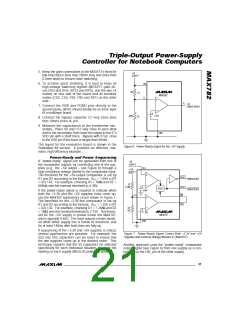
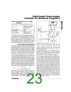
Figure 9. Simple Switching for PCMCIA Slot VCC
R2
390k
GND
+5V
FB5
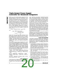
Figure 8. Power-Up Sequencing for the Intel 486SL
PCMCIA 2.0
DIGITAL
MAX782
Q1
N3
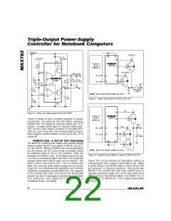
Figure 8 shows a more complex example of power
sequencing. On power-up, the Intel 486SL computer
requires the +5V supply to come up before the +3.3V
supply. A power-ready signal is required ≥50ms later.
This circuit’s ON3 output connects to the MAX782’s
ON3 pin, and can be wire-OR connected with an open-
drain output to enable another circuit to turn the +3.3V
supply off.
CONTROLLER
SLOT
VCC
+3.3V
FB3
Q2
VCC_EN0
VCC_EN1
D1
D2
N1
N2
100µF
P CMCIA S lo t +3 .3 V/+5 V VCC S w it c h in g
The MAX782 contains level shifters that simplify driving
external power MOSFETs to switch PCMCIA card VCC
to 3.3V and 5V. While a PCMCIA card is being inserted
into the socket, the VCC pins on the card edge should
be powered down to 0V so “hot insertion” does not
damage the PCMCIA card. The simplest way to do this
is to use a mechanical switch that has to be physically
opened before the PCMCIA card can be inserted. The
switch, which disconnects VCC, can be closed only
when the card has been fitted snugly into its socket.
Figure 9’s circuit illustrates this approach and correctly
shows the connections to both MOSFETs: N2 appears
to be inserted with drain and source the wrong way
around, but this is necessary to prevent its body diode
from pulling the +3.3V supply up to 5V when VCC is
connected to the +5V supply.
VH
VDD
NOTE: MOSFET BODY DIODES SHOWN FOR CLARITY.
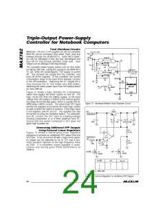
Figure 10. Using the Level Shifters to Switch PCMCIA Slot VCC
Figure 10’s circuit provides an alternative method of
connecting the VCC supply to the PCMCIA slot. While
it avoids using a mechanical switch, it does not provide
the security of a physical interlock. Placing the two
MOSFETs N1 and N2 with their body diodes facing in
opposite directions allows VCC to be shut down to 0V
without using a mechanical switch, and allows VCC to
be driven to 5V without the +3.3V supply being pulled
up to 5V.
22 ______________________________________________________________________________________

 MAXIM [ MAXIM INTEGRATED PRODUCTS ]