Functional Description
AU-AIS Insertion
Note that in case of a regenerator, all the received
MSOH bytes are passed through unchanged.
For both Terminal and ADM modes, it is possible to
force AU-AIS (“all one” into AU-3 or AU-4) via reg-
ister 30H.
B2 Error Byte(s):
The B2 (BIP-8 in STM-0 mode, BIP-24 in STM-1)
byte source is specified by register 70H and can come
from:
Test Points
Two output pins test points are available:
• MMSAJ1EN: This pulse (active High: pulse
duration is 51 ns (STM-1) or 154 ns (STM-0)
indicates J1 byte presence on the TB.
• Transmit Telecom bus (In ADM mode)
• By calculation on the previous frame
For testing purposes, it is possible to invert B2 value
(via register 71H). The B2 value can be inverted for a
single frame (8 errors) or for an indefinite duration.
• MMSAPAYEN: A High indicates the position of
VC-3 (STM-0) or VC-4 (STM-1) bytes. A Low
indicates the SOH + AU Pointer bytes presence
on the TB.
K1 and K2 Automatic Protection Channel
Bytes & MS-RDI:
These bytes are assigned for APS signaling and the
transmission of a Multiplex Section Remote Defect
Indication.
Transmit Multiplex Section Protection
(MSP Block)
This block is used in a 1-for-1 configuration (ADM or
Terminal). Two SXT6051 chips in parallel can trans-
mit the same AU data. In a non-protected configura-
tion, the data is simply passed to the transmit MST.
The K1 source is specified by the register 61H and can
come from:
• The serial RSOH and MSOH interface (TSOH
input pin)
In a 1-for-1 protection, one SXT6051 will be config-
ured as Master (Main) and the other one as Slave
(Redundant).
• An internal register (address 37H) programmed
by the microprocessor
The Master transmitter data flow follows the unpro-
tected mode flow and the SOH overhead will be added
in the Multiplexer Section Block.
The K2 source is specified by the register 61H:
• The serial RSOH and MSOH interface (TSOH
input pin)
In the Slave transmitter, the Higher Order Path Trans-
mitter and Pointer Processing block are not used. The
data and timing reference are input from the Master
transmitter to the Slave via the MSP bus. The Slave
Multiplexer and Regenerator Section Transmitter
blocks process these incoming AU data, clock and tim-
ing references.
• Internal hardware process. In this case the RDI
bits can be provided by RDI output from the
receiver (see Table 6) or an internal register
(address 38H) programmed by the microproces-
sor (in which case the other K2 bits are also
updated from register 38H). This choice is con-
figurable via register 30H
Note
The transmitted data at the Slave Regenerator
Section output (MHBDATA<7:0> or MHPOSD/
MHNEGD) is synchronized by the MSP bus
signal MMSPPJ0EN received from the Master.
This results in the A1 framing bytes of both
Master and Slave transmit frames being aligned.
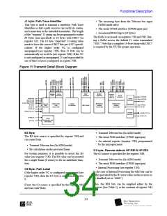
Multiplexer Section Transmitter
The multiplexer section inserts the MSOH overhead
bytes into the transmit frame.
36
l

 LevelOne [ LEVEL ONE ]