SXT6051 STM-1/0 SDH Overhead Terminator
(in which case the G1 spare bit is also sourced from
74H).
K3 Byte: APS
The K3 source is specified by the register 70H:
• The incoming byte from the Telecom bus input
(only in ADM mode).
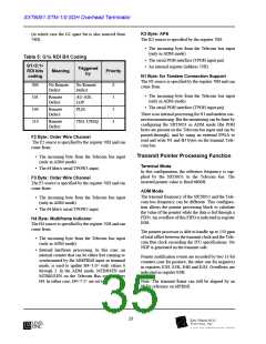
Table 5: G1x RDI Bit Coding
• The serial POH interface (TPOH input pin)
• An internal register (address 73H)
G1<3:1>
RDI bits
coding
Triggered
Meaning
Priority
by
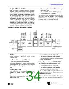
N1 Byte: for Tandem Connection Support
The N1 source is specified by the register 70H and can
come from:
000
101
100
110
No Remote
Defect
No Remote
Defect
0
1
2
3
• The incoming byte from the Telecom bus input
(only in ADM mode).
Remote
Defect
AU-AIS,
LOP
• The serial POH interface (TPOH input pin)
Remote
Defect
PLM
There is no internal processing for N1 and tandem con-
nection monitoring. But the monitoring can be done by
configuring the SXT6051 in ADM mode (the POH
bytes are present on the Telecom bus input and can be
passed-through), and by using an external FPGA to
read and write N1 and B3 bytes on the transmit Tele-
com bus.
Remote
Defect
TIM, UNEQ
F2 Byte: Order Wire Channel
The F2 source is specified by the register 70H and can
come from:
Transmit Pointer Processing Function
• The incoming byte from the Telecom bus input
(only in ADM mode).
Terminal Mode
• The 64 kbit/s serial TPOW1 input.
In this configuration, the reference frequency is sup-
plied by the SXT6051 to the Telecom bus. The
inserted pointer value is fixed 6800H.
F3 Byte: Order Wire Channel
The F3 source is specified by the register 70H and can
come from:
ADM Mode
The transmit frequency of the SXT6051 and the Tele-
com bus frequency can be different. This configura-
tion allows the pointer processing block to calculate
the value of the pointer while the data is fed through a
FIFO. An overflow of this FIFO is indicated in register
E0H.
• The incoming byte from the Telecom bus input
(only in ADM mode).
• The 64 kbit/s serial TPOW2 input.
H4 Byte: Multiframe Indicator
The H4 source is specified by the register 70H and can
come from:
The pointer processor is able to handle up to 150 ppm
of total offset between the transmit clock and the Tele-
com Bus clock exceeding the ITU specifications. No
NDF is generated on the transmit side.
• The incoming byte from the Telecom bus input
(only in ADM mode).
• Internal hardware processing. In this case, an
internal counter that can be either free running or
synchronized by the MMFRMI input in terminal
mode, is used to update H4<1:0> with values 0
through 3. In the ADM mode, MTBH4EN and
MTBJ0J1EN on the Telecom Bus synchronizes
H4. In either case, H4<7:2> are set to 1.
Pointer justification events are recorded by two 11-bit
counters (one for positive, the other one for negative)
in registers E2H, E3H, E4H and E5H. Overflows are
indicated in register E0H.
Note: The transmit frame can still be aligned by an
8KHz reference on MFRMI.
35

 LevelOne [ LEVEL ONE ]