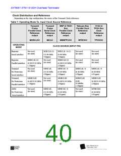
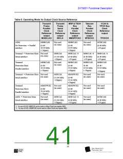
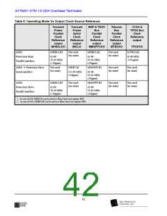
Functional Description
• The serial RSOH and MSOH interface (TSOH
input pin)
MFRMO of chip #2 connected to input pin MFRMI of
chip #3, etc.).
If the MFRMI is not used it must be tied to GND.
UN Bytes: Undefined Bytes
In the STM-1 mode, four “Undefined” bytes are
located in row number 2, column number 6 (UN2-6),
and in row number 3, column numbers 6 (UN3-6), 8
(UN3-8), and 9 (UN3-9) of the MSOH (see Figure 10).
Register 63H specifies the source of these bytes. The
possibilities are:
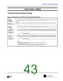
Parallel Interface
The parallel interface output is a byte wide bus MHB-
DATA. The parallel clock is output synchronous with
MHBCLKO (6.48 MHz/STM-0 or
19.44 MHz/STM-1).
• The received byte (Regenerator mode) from the
Regenerator Section receiver
The parallel interface is selected via register 50H. The
selection of a parallel interface is common between the
transmit and receive sides.
• The serial RSOH and MSOH interface (TSOH
input pin)
In case of a repeater application, the order on the par-
allel byte will be the same between the input and the
output and the delay is constant. The repeater delay is
approximately 700ns in STM-0 mode and 233ns in
STM-1 mode.
Scrambler
After inserting the RSOH bytes, the data is scrambled.
The ITU Standard scrambler is 27 -1. Two additional
scramblers 211 - 1 and 213 -1 can be programmed for
STM-0 and STM-1 via register 50H. This flexibility
allows the optimum choice of scrambler for a radio
application.
Serial Interface
The serial interface output at STM-0 is a B3ZS signal
output on MHPOSD and MHNEGD. The output clock
is MICLK (51.84 MHz).
The data scrambling can be disabled via register 50H
or via the external input pin SCRAMSEL.
Note that the selection of serial interface and B3ZS
decoder (see register 50H) is common to the transmit-
ter and the receive side of the chip.
External Frame Synchronization
The SXT6051 provides an external frame pulse refer-
ence (output pin MFRMO). It is an 8 KHz reference
signal with a pulse duration of 154ns (STM-0) or 51ns
(STM-1). This pulse is used to identify the position of
the frame start. This signal is synchronous with the
output transmit frame clock.
If the B3ZS decoder is not used, MHPOSD is used as
a NRZ output pin.
Transmit Frame Alignment
The transmit frame can be synchronized (in Terminal
or ADM mode, no protection or protection Master) by
using an external 8 KHz reference connected to the
MFRMI input pin. This input signal is active High and
can be either a square wave or a pulse.
If the SXT6051 is configured in parallel mode the
MFRMI input must be synchronous with the MHB-
CLKI parallel Transmit Frame clock reference input;
if the SXT6051 is configured in serial mode, the
MFRMI input must be synchronous with MHICLK
serial Transmit Frame clock reference input (51.84
MHz).
This feature can be used by an Upper Level Multi-
plexer to align several SXT6051s. The alignment can
done by cascading the reference signals (output pin
39
l

 LevelOne [ LEVEL ONE ]