Functional Description
J1 byte: Path Trace Identifier
• The incoming byte from the Telecom bus input
(ADM mode only)
This byte is used to transmit a repetitive Path Trace
Identifier so that a path receiver can verify its contin-
ued connection to the intended transmitter. The length
of the “transmit” J1 string can be programmed to either
64 bytes (non-specified) or 16 bytes with CRC7 via
register 71H. The 16 byte “expected” J1 string value
needs to have the correct CRC7 bits per G707 specifi-
cations. If the higher order VC is configured
unequipped (see register 71H), then J1 byte can be
automatically set to all 0s (see register 70H). If the VC
is not configured as unequipped, J1 can be provided by
one of three sources configured in register 70H:
• The serial TPOH interface (TPOH input pin)
• An internal RAM (up to 64 bytes)
The RAM is accessed via registers 75H and 76H. Dur-
ing a RAM access the default J1 value transmitted
“01H.” Note that a complete 16-byte string with CRC7
is required by the ITU for proper operation.
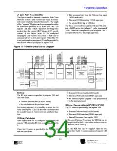
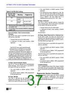
Figure 11:Transmit Detail Block Diagram
MSP
Interface
MSOH
Interface
SERIAL
TPOH
TPOH
Interface
SERIAL
RSOH
&MSOH
RSOH
Interface
M HNEGD
M HPOSD
M ICLK
Serial
Interface
M TBH4EN
M TBPAYEN
M TBJ0J1EN
M TBTUGEN
1 TO 3
Telecom
Bus
Interface
Higher order
Path
Transmitter
Pointer
Processing
Multiplexer
section
Transmitter
Regenerator
Section
Transmitter
M TBCKI
M TBCKO
M TBPAR
M FRMO
M FRMI
MSP Block
M TBDATA<7:0>
Parallel
M HBDATA<7:0>
M HBCLKO
Interface
M HBCLKI
M HICLK
Clock
Distribution and
References
B3 Byte
• Transmit Telecom bus (In ADM mode)
• The serial POH interface (TPOH input pin)
The B3 byte source is specified by register 70H and
can come from:
• An internal register (register 72H) programmed
by the microprocessor
• Transmit Telecom bus (In ADM mode)
• By calculation on the previous frame
G1 byte: Remote defects HP-REI & HP-RDI
For testing purposes, it is possible to invert the B3
value (see register 71H). The B3 value can be inverted
for a single frame (8 errors) or for an indefinite dura-
tion.
The G1 source is specified by the register 70H:
• Transmit Telecom bus (In ADM mode)
• The serial POH interface (TPOH input pin)
• Internal Processing (see register 71H)
C2 Byte: Path Label
If the higher order VC is configured unequipped (see
register 71H), then the C2 byte is automatically set to
0.
In the case of Internal Processing the REI bits can be
either provided by the B3 error value on the receiver or
be disabled (set to “0000”).
Also, the RDI bits can be supplied either by the
receiver (See Table 5), or the contents of register 74H
If not, the C2 source is specified by the register 70H
and can come from:
34
l

 LevelOne [ LEVEL ONE ]