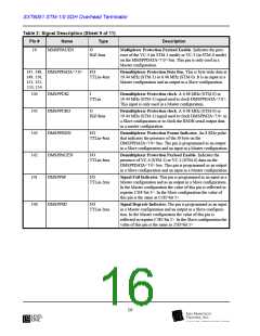
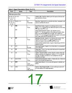
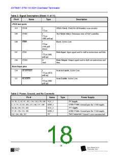
Functional Description
FUNCTIONAL DESCRIPTION
Thus both transmitters are synchronous in a 1-for-1 hot
stand-by configuration.
Transmit Data Flow
Figure 2 shows the functional blocks of the SXT6051. For
the transmitter (lower half of the diagram), the input inter-
face is the Multiplexer Telecom Bus with byte wide data
MTBDATA <7:0> and timing signals for the parallel clock
MTBCK, the frame indicator MTBJ0J1EN, and the pay-
load active signal MTBPAYEN. The MTBPAR signal pro-
vides parity checking on the MTBDATA <7:0> byte data.
Next, the MST function adds the Multiplexer Section
OverHead (MSOH):
• The K1 and K2 bytes are sourced from the micropro-
cessor programmable register or TSOH input. In the
particular case of K2, an internal process inserts the
MS-RDI bits (K2<2:0>) based on the receive infor-
mation if automatic MS-RDI insertion is enabled by
the microprocessor.
The data flow starts with the Higher Order Path Termina-
tion section which adds the VC-3 or VC-4 path overhead:
• The D4-D12 bytes are sourced from the TMD input or
received D4-D12 bytes in ADM mode. A 576 KHz
reference clock is supplied at TMDC.
• The 16 or 64 byte J1 string is sourced from the micro-
processor programmable registers or TPOH input.
The microprocessor must calculate the CRC7 byte of
the 16 byte J1 transmit string and store it in the first
byte of the registers storing the string.
• S1 is sourced from the microprocessor programmable
register or TSOH input.
• M1 is sourced from the TSOH input or an internal
process that sets M1 based on the receive B2 byte(s)
errors from the receive portion of the SXT6051 if
automatic MS-REI insertion is enabled by the micro-
processor.
• The B3 byte is calculated internally and inserted. The
microprocessor can invert the values of B3 for system
testing purposes.
• The C2 byte is sourced from the microprocessor pro-
grammable register or TPOH input.
• E2 is sourced from the TMOW input or, in ADM
mode, received E2 byte. A 64 KHz reference clock is
supplied at TROWC and an 8 KHz sync pulse at
TROWBYC.
• The G1 byte is sourced from the microprocessor pro-
grammable register, TPOH input, or from the receive
portion of the chip if automatic RDI and REI insertion
is enabled by the microprocessor
• The B2 byte is calculated internally and inserted. The
microprocessor can invert the values of B2 for system
testing purposes.
• The F2 and F3 bytes are two 64 Kbit/s channels
sourced from TPOW1 and TPOW2 or the received F2
and F3 bytes. TPOWC (at 64 KHz) and TPOWBYC
(at 8 KHz) provide the timing references for these
channels.
Finally, the Regenerator Section OverHead (RSOH) is
added by the Regenerator Section Termination (RST).
• The K3 byte is sourced from the microprocessor pro-
grammable register or TPOH input.
• J0 byte is sourced from the microprocessor, TSOH
input or received J0 byte. The microprocessor must
calculate the CRC7 byte of the J0 transmit string and
store it in the first byte of the registers storing the
string.
After the HPOH data has been added, the Higher Order
Connection Supervision block can insert an “unequipped”
payload if configured by the microprocessor to do so (see
registers 70H and 71H).
• The B1 byte is calculated internally and inserted. The
microprocessor can invert the values of B1 for system
testing purposes.
Pointer processing re-timing is performed by the Multi-
plexer Section Adaptation (MSA) section. Positive and
negative pointer movement events are stored in counters
that can be accessed via the microprocessor interface. The
resulting parallel data stream is supplied to the Multiplexer
Section Termination (MST) and to the Multiplexer Section
Protection (MSP) port if it is configured as a protection
master. The data MMSPPDATA <7:0>, along with timing
information, is sent to the redundant (slave) SXT6051.
• E1 is sourced from the TROW input or, in ADM
mode, received E1 byte. A 64 KHz reference clock is
supplied at TROWC and an 8 KHz sync pulse at
TROWBYC.
19
l

 LevelOne [ LEVEL ONE ]