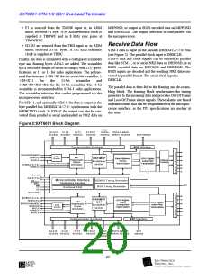
Functional Description
After frame synchronization and de-scrambling, the
Regenerator Section Termination (RST) extracts the
RSOH:
“Master MST output data” or “Slave MSP output data” (see
figure 6 or section on page 31). The choice is completely
under the control of the microprocessor. The microproces-
sor has access to all the Master and Slave data (K1/K2
bytes, error statistics derived from counters and alarm sta-
tus from both chips) necessary for making this decision.
• The expected value of the J0 string is stored via the
microprocessor interface. The received J0 string is
compared with the stored version, and also used to
calculate a CRC-7 byte. Two alarms can be generated:
a J0 (Trace ID) Mismatch alarm and J0 CRC-7 mis-
match alarm.
The MSA block interprets the H1-H3 payload points bytes
to determine the location of the VC-3 or VC-4 payload
structure. Positive and negative pointer movement events
are stored in counters that can be accessed via the micro-
processor interface. The data from the MSA section is then
output to the HPT section in a byte parallel format.
• B1 byte is calculated internally and compared to the
incoming B1 value. The errors are stored into a set of
counters that can be read by the microprocessor inter-
face.
The HPT section extracts the HPOH:
• E1 is provided serially at the RROW output.
• The expected value of the 16 on 64 byte J1 string is
stored internally via the microprocessor interface. The
receive value of J1 is compared with the stored ver-
sion, and is also used to calculate a CRC-7 byte (in 16
byte string configuration). Two alarms are generated:
a J1 Mismatch alarm and J1 CRC-7 mismatch alarm.
• B3 byte is calculated internally and compared to the
incoming B3 value. The errors are stored into a set of
counters that can be read by the microprocessor inter-
face. These errors are also inserted in the transmitted
G1 REI bits (G1<7:4>) if enabled (see registers 70H
and 71H).
• F2 and F3 are provided serially at the ROW1 and
ROW2 outputs. The 64 KHz clock reference for this
output is provided at RPOWC and the 8 KHz sync
pulse at RPOWBYC.
• C2 is provided via both a microprocessor register and
serially at the RPOH output. The C2 value provided
via a microprocessor register is filtered over 3 or 5
frames. The number of filtering frames can be pro-
grammed by the microprocessor.
• G1 is provided serially at the RPOH and is used to
update HPTREI-CNT registers accessible by the
microprocessor.
• K3 is provided via both a microprocessor register and
serially at the RPOH output.
The last block is the re-timing block. This block allows the
alignment of the receive payload with the external signal
DRETFRMI, which supplies the J0 position and an exter-
nal clock DRETCLK. A new value of the pointer based on
the new alignment position is assigned to the payload. This
block typically is bypassed for a multiplexer application. It
is typically only required for external re-timing and align-
ment of multiple TUG-3 payload signals.
• F1 is provided serially at the RMOW output. E1 and
F1 are synchronous and can be accessed using the 64
KHz clock provided at RROWC and the 8 KHz syn-
chronization pulse provided at RROWBYC.
• D1-D3 are provided serially at the RRD output. The
192 KHz clock reference for this output is provided at
RRDC.
Next the Multiplexer Section Termination (MST) extracts
the MSOH:
• K1 and K2 bytes are provided via both a microproces-
sor register and serially at the RSOH output. A filter
based on 3 consecutive identical values of K1 and K2
gates the update of the microprocessor registers.
• D4-D12 bytes are provided serially at the RMD out-
put. The 576 KHz clock reference for this output is
provided at RMDC.
• S1 is provided via both a microprocessor register and
serially at the RSOH output. A filter based on 3 con-
secutive identical values of S1 gates the update of the
microprocessor register.
• M1 is provided serially at the RSOH output and
updates MST REI counters accessible by the micro-
processor.
• E2 is provided serially at the RMOW output. The
64 KHz clock reference for this output is provided at
RROWC and the 8 KHz sync pulse at RROWBYC.
• B2 byte is calculated internally and compared to the
incoming B2 value. The errors are stored into a set of
counters that can be read by the microprocessor inter-
face. These errors are also inserted in the transmitted
M1 byte if enabled (see register 60H).
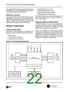
The Multiplexer Section Protection (MSP) block allows
the selection of data presented to the Master Multiplexer
Section Adaptation (MSA) block to come from either the
21
l

 LevelOne [ LEVEL ONE ]