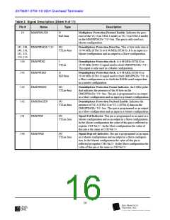
SXT6051 Pin Assignments And Signal Description
Table 2: Signal Description (Sheet 8 of 11)
Pin # Name Type
Description
103, 102, DTBDATA<7:0>
O
Demultiplexer Telecom Bus Data. This is a byte wide data
output at 19.44 Mb/s for STM-1 or 6.48 Mb/s for STM-0. The
RSOH, MSOH and HPOH values are present on the bus when
receive re-timing is disabled (see register 51H).
101, 100,
99, 98, 97,
96
HiZ-4ma
94
93
92
91
DTBPAR
O
Demultiplexer Telecom Bus Parity. A parity check calculated
on each output byte on the Telecom Bus. It is an odd parity.
HiZ-4ma
DTBCK
O
Demultiplexer Telecom Bus Clock Output. A 6.48MHz
(STM-0) or 19.44 MHz (STM-1) output signal.
HiZ-8ma
DTBJ0J1EN
DTBTUGEN1
O
Demultiplexer Telecom Bus Frame Indicator. It indicates the
presence of J0 and J1 bytes on the receive telecom bus.
HiZ-4ma
O
Demultiplexer Telecom Bus Payload Enable 1. Indicates the
presence of TUG3#1 in the case of STM-1. In the case of
STM-0 this pin is internally pulled High.
HiZ-4ma
90
89
DTBTUGEN2
DTBTUGEN3
O
Demultiplexer Telecom Bus Payload Enable 2. Indicates the
presence of TUG3#2 in the case of STM-1. In the case of
STM-0 this pin is internally pulled High.
HiZ-4ma
O
Demultiplexer Telecom Bus Payload Enable 3. Indicates the
presence of TUG3#3 in the case of STM-1. In the case of STM-
0 this pin is internally pulled High.
HiZ-4ma
88
87
DTBPAYEN
DTBH4EN
O
Demultiplexer Telecom Payload Enable. Indicates the pres-
ence of VC-4 in the STM-1 mode or VC-3 in the STM-0 mode.
HiZ-4ma
O
Demultiplexer Multi-Frame Indicator. A 2 KHz signal that
HiZ-4ma
indicates a value of “00” for H4.
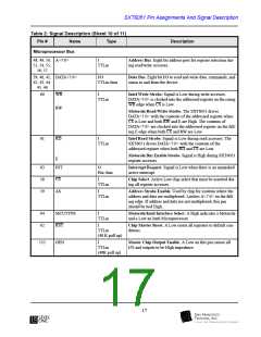
Multiplexer/Demultiplexer Protection Interface
9, 8, 7, 6, MMSPPDATA<7:0> I/O
Multiplexer Protection Data Bus. This is byte wide data at
19.44 Mb/s for STM-1 or 6.48 Mb/s for STM-0. It is an output
when the SXT6051 is a Master in a 1-for-1 protection. It is an
input when the SXT6051 is a Slave in a 1- for-1 protection.
5, 4, 3, 2
TTLin-4ma
11
MMSPPCKI
MMSPPCKO
I
Multiplexer Protection Clock. A 6.48MHz (STM-0) or 19.44
MHz (STM-1) input signal used to clock MSPPDATA<7:0>.
This input is only used when the SXT6051 is configured as
Slave in a 1-for-1 protection.
TTLin
12
13
O
Multiplexer Protection Clock A 6.48MHz (STM-0) or 19.44
MHz (STM-1) output signal used to clock MSPPDATA<7:0>.
This output is used when the SXT6051 is configured as Master
in a 1-for-1 protection. This clock is also used to clock the
TSOH serial data stream.
HiZ-8ma
MMSPPJ0EN
I/O
TTLin-4ma
Multiplexer Protection Frame Indicator An 8 KHz pulse
that indicates the presence of the J0 byte on
MMSPPDATA<7:0> bus. The pin is programmed as an input
in a Slave configuration and an output in a Master configura-
tion.
15

 LevelOne [ LEVEL ONE ]