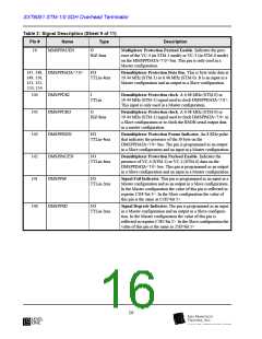
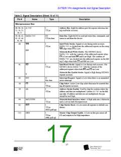
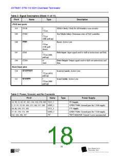
SXT6051 STM-1/0 SDH Overhead Terminator
• F1 is sourced from the TMOW input or, in ADM
mode, received F1 byte. A 64 KHz reference clock is
supplied at TROWC and an 8 KHz sync pulse at
TROWBYC.
MHPOSD, or output as B3ZS encoded data on MHPOSD
and MHNEGD. The output selection is configurable via
the microprocessor.
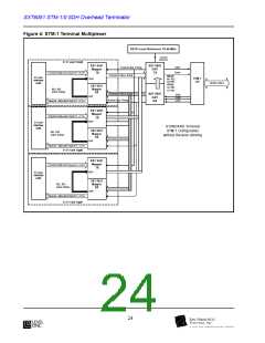
Receive Data Flow
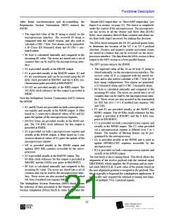
• D1-D3 are sourced from the TRD input or, in ADM
mode, received D1-D3 bytes. A 192 KHz reference
clock is supplied at TRDC.
STM-1 data is input on the parallel DHBDATA<7:0> bus
(see Figure 2). The parallel clock input is DHBCLK.
STM-0 data and clock signals can be entered as parallel
data like STM-1, or as serial NRZ data on DHPOSD, or as
B3ZS encoded data on DHPOSD and DHNEGD. The
B3ZS inputs are decoded and the resulting NRZ data con-
verted to parallel format. The serial clock input is
DHICLK.
Finally, the data is scrambled with a configured scrambler
type and framing bytes A1/A2 are added. The scrambler
has a selectable length of seven to comply with ITU speci-
fications, or 11 or 13 for radio applications. The polyno-
mial functions are 1+X6+X7 for the seven-bit scrambler, 1
+X9+X11
for
the
11-bit
scrambler
and
1+X8+X9+X12+X13 for the 13-bit scrambler. The 13-bit
scrambler is recommended for STM-1 radio applications.
The scrambler selection that can be programmed via the
microprocessor interface.
The parallel data is then fed to the framing and de-scram-
bling block. The framing block synchronizes the timing
generator to the incoming data and provides Out Of Frame
and Loss Of Frame alarm signals. These alarms are based
on frame counts that can be programmed via the micropro-
cessor interface, as the ITU specifications are unclear at
this time.
For STM-1, and optionally STM-0, the data is output on the
byte parallel bus MHBDATA<7:0> synchronous with the
MHBCLKO clock. In STM-0, the output can also be con-
verted from parallel to serial and emitted as NRZ data on
Figure 2:SXT6051 Block Diagram
HPOH
SERIAL
ACCESS SERIAL ACCESS
D4 D12
ACCESS ACCESS
D1 D3
F2 F3
ACCESS
E1 E2 F1
ACCESS
RSOH & M SOH
M SP interface
Com m unication O verhead
MSP Interface
DHPOSD/DHNRZ
DHNEGD
B3ZS
Decoder
RST
MST/MSP
Demultiplexer
Pointer
Interpretation
HOA Higher
order Path
Termination
Regenerator
M ultiplexer
Section
term ination
Retiming
Function
DHICLK
section
DHBDATA<7:0>
DHBCLK
A<7:0>
DATA<7:0>
M icrocontroller Interface
DE M U X Tim ing G enerator
M UX Tim ing G enerator
W R/RW
RD/E
CS
Intel/Motorola Selectable
RST
O verhead R AM
AS
M CUTYPE
M HBDATA<7:0>
M HBCLKO
MSA/MSP
MST
M ultiplexer
section
HCS Higher
order
Connection
Supervision
RST
Regenerator
Section
term ination
HOA Higher
order Path
Termination
M HPOSD/MHNRZ
M HNEGD
M ICLK
B3ZS
Encoder
M HBCLK
M HICLK
Com m unication O verhead
MSP Interface
D4 D12
ACCESS ACCESS
D1 D3
F2 F3
ACCESS
E1 E2 F1
ACCESS
HPOH
SERIAL
ACCESS
RSOH & M SOH
SERIAL ACCESS
M SP
Interface
20

 LevelOne [ LEVEL ONE ]