SXT6051 Pin Assignments And Signal Description
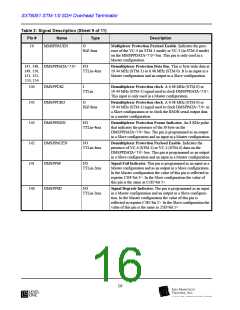
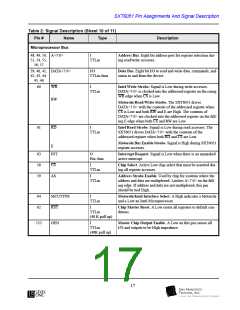
Table 2: Signal Description (Sheet 10 of 11)
Pin # Name Type
Description
Microprocessor Bus
48, 49, 50, A<7:0>
51, 54, 55,
I
Address Bus. Eight bit address port for register selection dur-
ing read/write accesses.
TTLin
56, 57
39, 40, 41, DATA<7:0>
42, 43, 44,
I/O
TTLin-6ma
Data Bus. Eight bit I/O to read and write data, commands, and
status to and from the device.
45, 46
60
WR
RW
I
Intel Write Strobe. Signal is Low during write accesses.
DATA<7:0> is clocked into the addressed register on the rising
WR edge when CS is Low.
TTLin
Motorola Read/Write Strobe. The SXT6051 drives
DATA<7:0> with the contents of the addressed register when
CS is Low and both RW and E are High. The contents of
DATA<7:0> are clocked into the addressed register on the fall-
ing E edge when both CS and RW are Low.
61
RD
I
Intel Read Strobe. Signal is Low during read accesses. The
SXT6051 drives DATA<7:0> with the contents of the
addressed register when both RD and CS are Low.
TTLin
Motorola Bus Enable Strobe. Signal is High during SXT6051
register accesses.
E
63
58
59
INT
O
Interrupt Request. Signal is Low when there is an unmasked
active interrupt.
Hiz-4ma
CS
AS
I
Chip Select. Active Low chip select that must be asserted dur-
ing all register accesses.
TTLin
I
Address Strobe Enable. Used by chip for systems where the
address and data are multiplexed. Latches A<7:0> on the fall-
ing edge. If address and data are not multiplexed, this pin
should be tied High.
TTLin
64
62
MCUTYPE
RST
I
Motorola/Intel Interface Select. A High indicates a Motorola
and a Low an Intel Microprocessor.
TTLin
I
Chip Master Reset. A Low resets all registers to default con-
TTLin
ditions.
(48 K pull up)
155
OEN
I
Master Chip Output Enable. A Low on this pin causes all
TTLin
I/O and outputs to be High impedance.
(48K pull up)
17

 LevelOne [ LEVEL ONE ]