LTC1698
W U U
APPLICATIO S I FOR ATIO
U
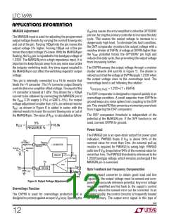
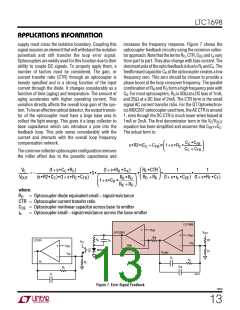
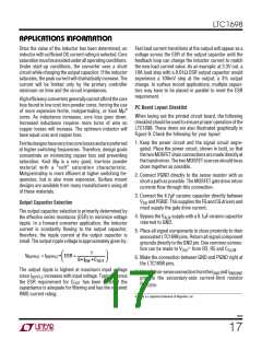
increases the frequency response. Figure 7 shows the
optocoupler feedback circuitry using the common collec-
tor approach. Note that the terms RD, CTR, CDE and rπ vary
from part to part. They also change with bias current. The
dominantpoleoftheoptofeedbackisduetoRF andCF.The
feedforward capacitor CK at the optocoupler creates a low
frequency zero. This zero should be chosen to provide a
phase boost at the loop crossover frequency. The parallel
combination of RK and RD form a high frequency pole with
CK. For most optocouplers, RD is 50Ω at a DC bias of 1mA,
and 25Ω at a DC bias of 2mA. The CTR term is the small
signal AC current transfer ratio. For the QT Optoelectron-
ics MOC207 optocoupler used here, the AC CTR is around
1, even though the DC CTR is much lower when biased at
1mA or 2mA. The first denominator term in the VC/VOUT
equation has been simplified and assumes that CFB<<CC.
The actual term is:
supply must cross the isolation boundary. Coupling this
signal requires an element that will withstand the isolation
potentials and still transfer the loop error signal.
Optocouplers are widely used for this function due to their
ability to couple DC signals. To properly apply them, a
number of factors must be considered. The gain, or
current transfer ratio (CTR) through an optocoupler is
loosely specified and is a strong function of the input
current through the diode. It changes considerably as a
function of time (aging) and temperature. The amount of
aging accelerates with higher operating current. This
variation directly affects the overall loop gain of the sys-
tem. Tobeaneffectiveopticaldetector, theoutputtransis-
tor of the optocoupler must have a large base area to
collect the light energy. This gives it a large collector to
base capacitance which can introduce a pole into the
feedback loop. This pole varies considerably with the
current and interacts with the overall loop frequency
compensation network.
CC •CFB
s•R2•(CC + CFB)• 1+ s•RC •
CC + CFB
Thecommoncollectoroptocouplerconfigurationremoves
the miller effect due to the parasitic capacitance and
VC
VOUT
(1+ s•CC •RC)
(s•R2•CC)•(1+ s•RC •CFB)
(1+ s•RK •CK)
RF •CTR
1
1
= –
•5•
•
•
•
RD + RK (1+ s•r •CDE) (1+ s•RF •CF)
π
RK •RD
1+ s•CK •
RK + RD
where:
RD = Optocoupler diode equivalent small− signalresistance
CTR = Optocoupler current transfer ratio
CDE = Optocoupler nonlinear capacitor across base to emitter
r
π
= Optocoupler small− signalresistance across the base emitter
LTC1698
+
V
REF
20k
V
OPTODRV
OUT
+
–
V
REF
R
R2
C
K
K
LT3781
–
V
CC
V
FB
100k
+
–
V
REF
MOC207
R1
V
COMP
V
FB
C
C
R
C
V
C
R
E
C
FB
R
F
1698 F07
C
F
Figure 7. Error Signal Feedback
1698f
13

 Linear [ Linear ]